The nanoFAB supports two lithography processes – Photolithography & Electron Beam Lithography.
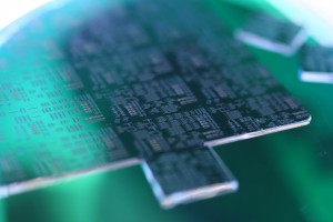
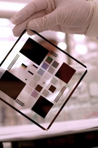
Photolithography, also termed optical lithography or UV lithography, is a process used in microfabrication to pattern parts of a thin film or the bulk of a substrate. It uses light to transfer a geometric pattern from a photomask to a light-sensitive chemical “photoresist“, or simply “resist,” on the substrate. A series of chemical treatments then either engraves the exposure pattern into, or enables deposition of a new material in the desired pattern upon, the material underneath the photo resist. For example, in complexintegrated circuits, a modern CMOS wafer will go through the photolithographic cycle up to 50 times.
Photolithography shares some fundamental principles with photography in that the pattern in the etching resist is created by exposing it to light, either directly (without using a mask) or with a projected image using an optical mask. This procedure is comparable to a high precision version of the method used to make printed circuit boards. Subsequent stages in the process have more in common with etching than with lithographic printing. It is used because it can create extremely small patterns (down to a few tens of nanometers in size), it affords exact control over the shape and size of the objects it creates, and because it can create patterns over an entire surface cost-effectively. Its main disadvantages are that it requires a flat substrate to start with, it is not very effective at creating shapes that are not flat, and it can require extremely clean operating conditions.
Electron-beam lithography, often abbreviated as e-beam lithography or EBL, is the practice of emitting a beam of electrons in a patterned fashion across a surface covered with a film (called the resist),[1] (“exposing” the resist) and selectively removing either exposed or non-exposed regions of the resist (“developing”). The purpose, as with photolithography, is to create very small structures in the resist that can subsequently be transferred to the substrate material, often by etching. It was developed for manufacturing integrated circuits, and is also used for creating nanotechnology architectures.
The primary advantage of electron-beam lithography is that it is one of the ways to beat the diffraction limit of light and make features in the nanometre regime. This form of maskless lithography has found wide usage in photomask-making used in photolithography, low-volume production of semiconductor components, and research & development.
The key limitation of electron-beam lithography is throughput, i.e., the very long time it takes to expose an entire silicon wafer or glass substrate. A long exposure time leaves the user vulnerable to beam drift or instability that may occur during the exposure. Also, the turnaround time for reworking or re-design is lengthened unnecessarily if the pattern is not being changed the second time.
The nanoFAB offers software tools for script generation of EBL patterns (Raith_GDSII) and 3D simulation of the exposure and development processes of electron-beam resists (EBL Simulator).

