


The Beginning - 1999
The Beginning
The nanoFAB originates from a long history of diligent and dedicated research efforts from a diverse group of professors. Seeing the potential of a multidisciplinary research facility in allowing for exceptional collaborations and shared resources the “MicroFab” was conceived April 1999.
In 1999, the MicroFab was housed in a small, old lab in the Newton Research Building, which has since been torn down and replaced by the Katz Building. Although we had very big aspirations – or very small – we had very few microfabrication capabilities, in a 2400 square foot space, with only $500 000 worth of equipment and facility infrastructure, managed by a staff of one.
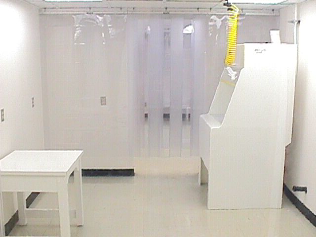
An Early Photolithography Station
Growing and a New Facility - 2001
Growth and a New Facility
Since these humble beginnings we have seen tremendous growth in both the user community and our capabilities. Our vision was to have an “Open Access Facility”, having world class scientists and researchers from both academia and industry working alongside undergraduate, summer & graduate students.
In 2001 the nanoFAB found a new home in the newly constructed Electrical & Computer Engineering Research Facility (ECERF). The facility was moved into a purpose built space consisting of approx 3500 sq feet of class 1000 cleanroom space (although we regularly meet class 10 specifications), and an additional 1300 sq feet of class 10k space housing various deposition, characterization and other equipment.
The Micromachining and Nano Fabrication (nanoFAB ) has proven to be a great learning environment for students as well as a flexible working environment for researchers and industrial users. Together, working side by side, we can achieve unique collaborations for research and training of the workforce of tomorrow.
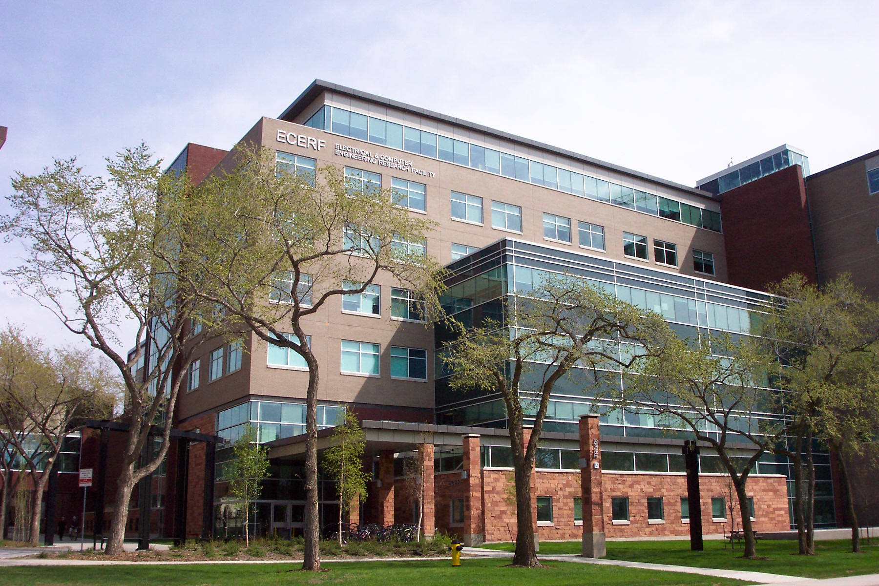
Our New Home in ECERF
Moving Forward - 2013
Moving Forward
As the University changes to meet the reality of challenges in the new economic landscape, the nanoFAB is changing as well. Consolidation of resources has enabled us to provide a wider range of services & capabilities to our user community, with the amalgamation of the equipment and expertise from several other facilities. This has brought on a suite of characterization capabilities, as well as a high performance computing cluster, now accessed through a single external interface.
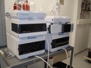
New Characterization Equipment (Agilent 1290 HPLC)