The nanoFAB is pleased to announce the following three positions at iscpi.
Semiconductor Packaging Engineer - Own the packaging solution for MEMS devices from concept to qualification (dicing, die attach, interconnect). Mostly supplier engagement, some cleanroom.
Semiconductor Microfabrication Engineer - Build the fabrication processes for our MEMS devices and AFM probe tips, from concept through qualification. Mix of cleanroom and supplier work.
R&D Application Engineer - Develop characterization protocols for customer samples and push AFM hardware to its limits through novel drive methods, calibration, and data analysis.
For more information about these listings and other job openings, please visit www.icspicorp.com/careers.
About icspi
icspi is building the future of nanoscale imaging.
We’ve revolutionized atomic force microscopy (AFM) by miniaturizing it by a factor of 1,000,000× compared to traditional systems: integrating all the components of an AFM onto a single CMOS chip, which we call microAFM.
Our core tech is field-proven and powers our desktop instruments that are used by scientists and engineers in over 40 countries.
Now we are using our core tech to solve throughput-resolution gaps in the semiconductor industry: catching nanoscale defects to enable new processes and prolong Moore's Law.
Today, scanning a wafer with AFM would take about 70 years. By using thousands of microAFMs in parallel, we can scan a wafer in a matter of hours.
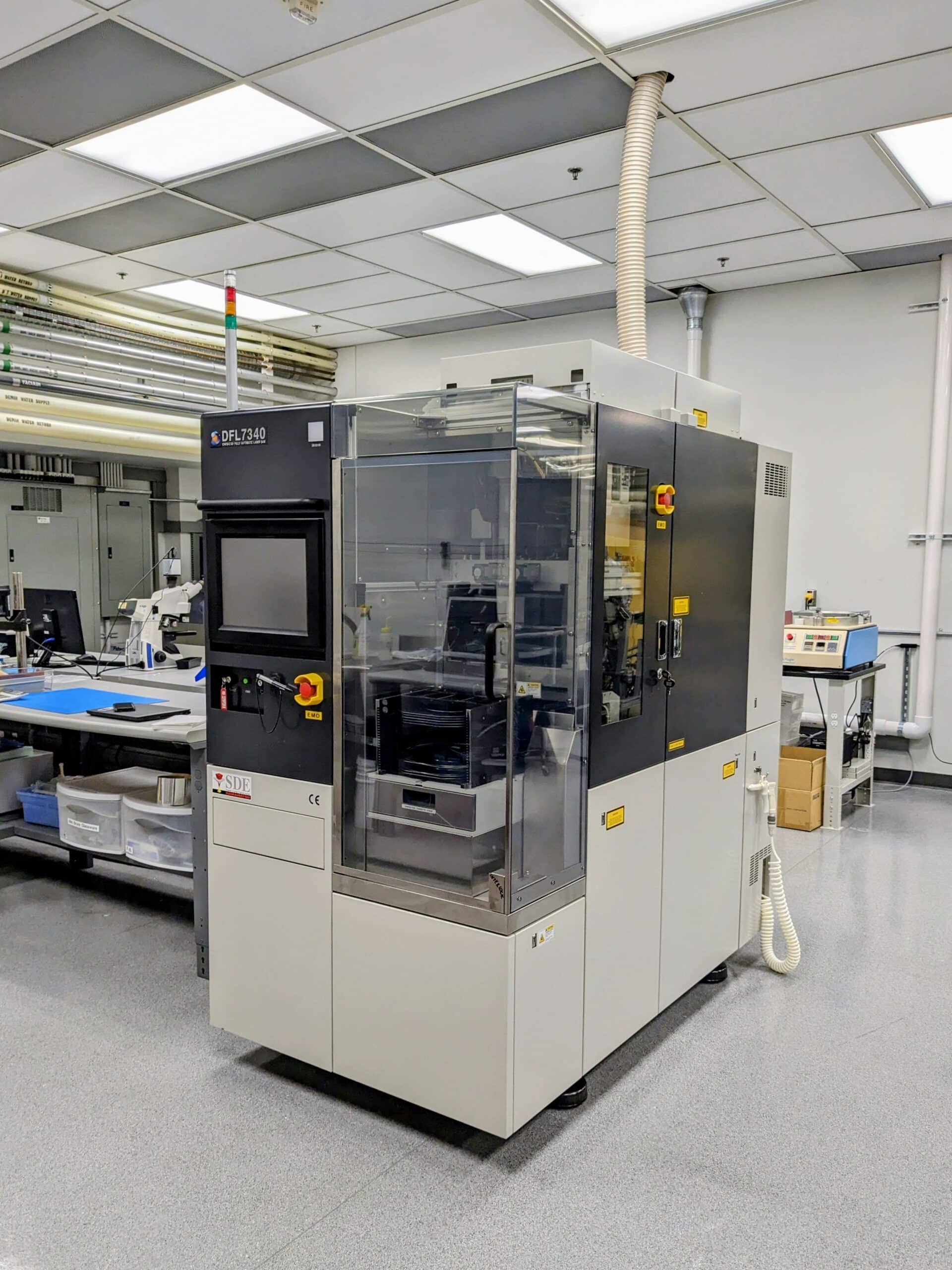
The nanoFAB is happy to announce the installation of a Disco DFL7340 Stealth Dicer into our 10k cleanroom space—only the second tool of its kind in Canada. Compared to mechanical dicing, stealth dicing has substantially less chipping and is able to "cut" dry. With no water present, MEMS wafers or other sensitive substrates can now be safely diced at the end of their processing, without the need for a photoresist layer to protect the surface. Our DFL7340 is equipped with a SDE03 stealth dicing engine, dedicated to dicing Si substrates only.
The Disco DFL7340 stealth dicer
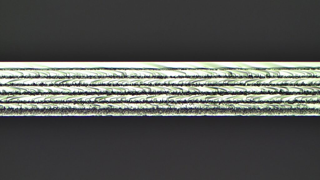
The stealth dicing process uses a ns-pulsed near infrared laser to create subsurface lines of voids and microcracks within the bulk Si; several lines at different depths and powers are typical in an optimised recipe. Crack propagation from these laser-modified lines singulate the wafer into individual dies—in this way, stealth dicing is more akin to "controlled cleaving" than sawing, with next to no material being removed from the dicing street (kerf loss). Compared to mechanical dicing, with its typical blade kerfs of 10s to 100s of µm, stealth dicing can therefore produce substantially less cutting waste, which in some cases can allow for more dies to be fit on a wafer. This process is also appropriate for samples that may be susceptible to contamination, as fewer particles are generated during stealth dicing vs. mechanical dicing.
Cross-sectional image of a 525 µm thick Si wafer after stealth dicing. Note that 6 passes were used to singulate a wafer of this thickness.
After dicing, a die expander is used to separate the dies after singulation to allow for "chipping-free" dies.
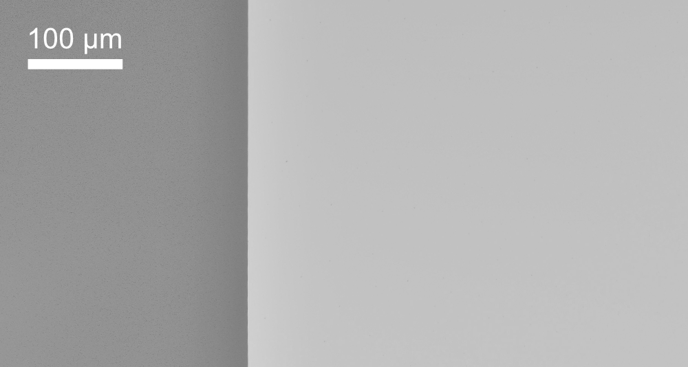
Edge quality of a Si chip after stealth dicing: note the nearly perfect edge and lack of contamination.
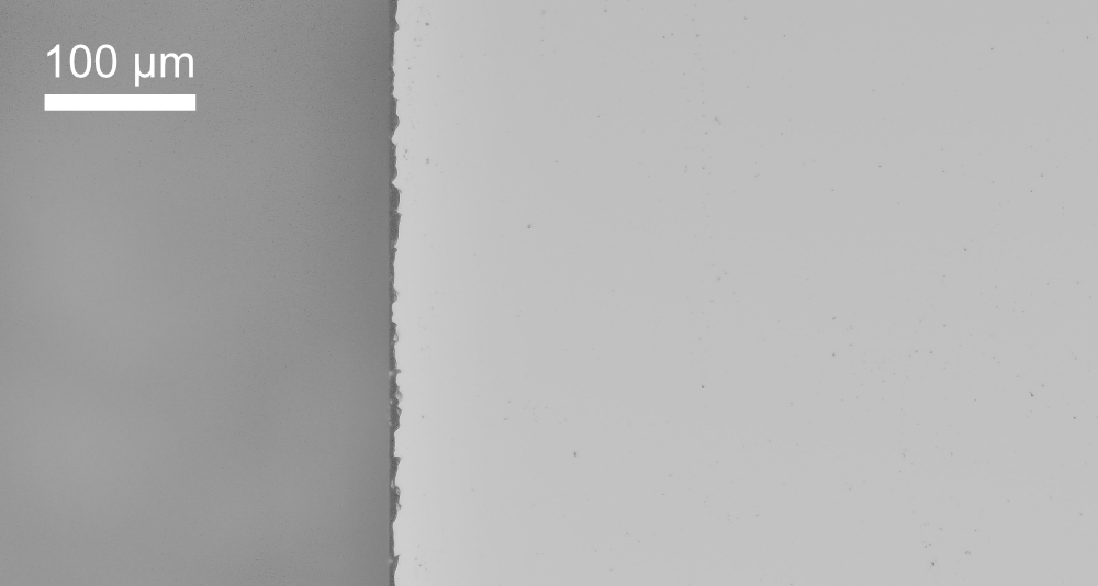
Edge quality of a Si chip after mechanical dicing: note the chipping and contamination (particles).
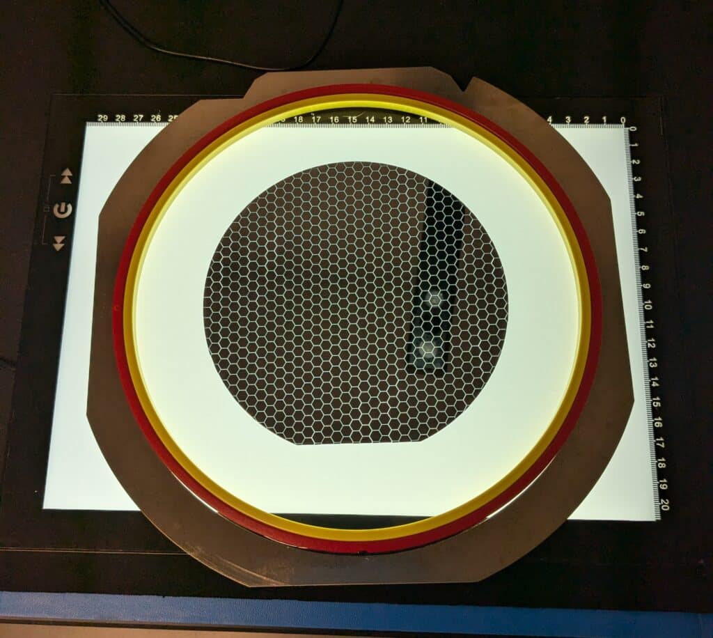
Wafer Expansion
Typically, for a well-optimised recipe, the dies are already fully singulated after the stealth dicing process. With near-zero kerf loss, however, the dicing lines are not easily seen until after the tape is expanded.
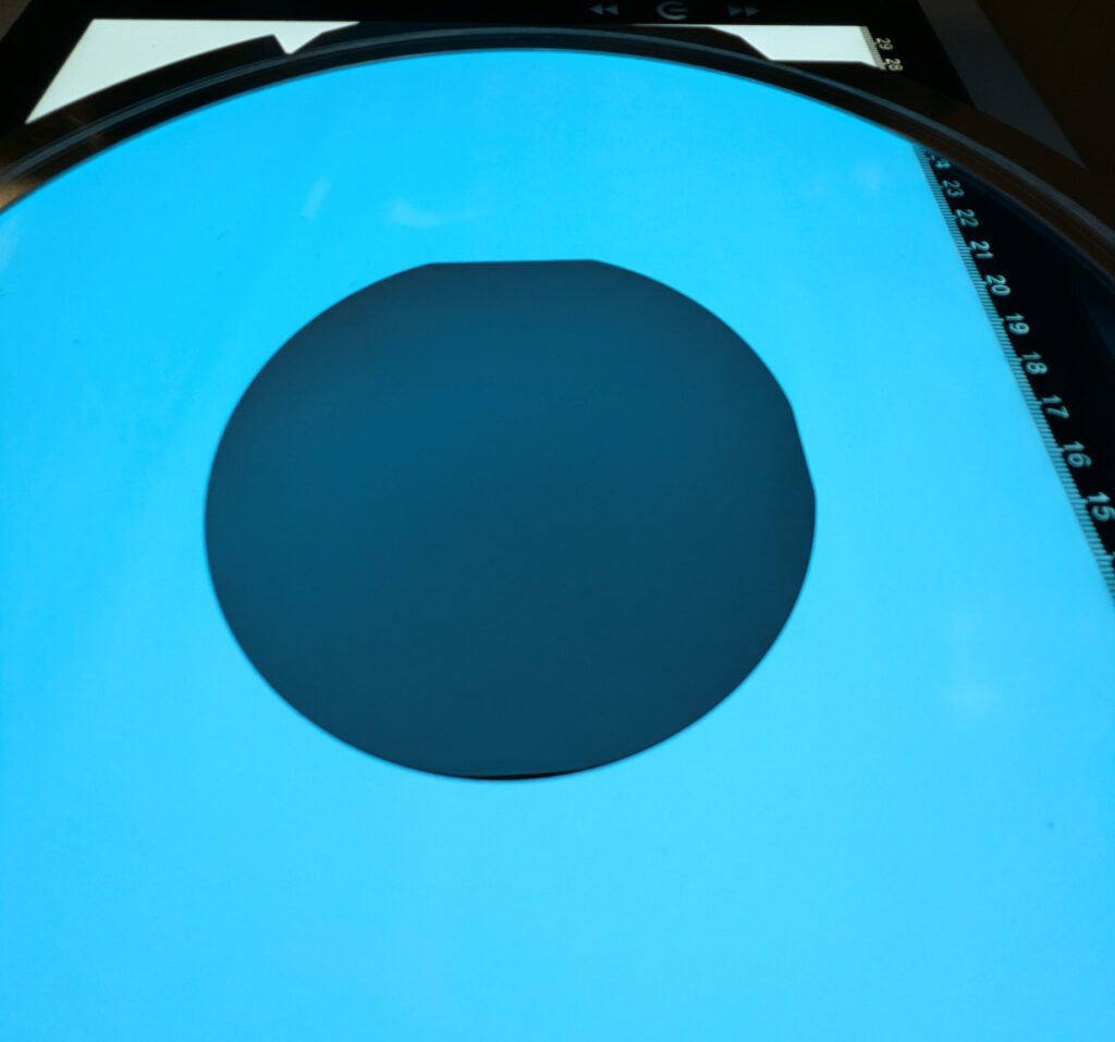
100 mm Si wafer after stealth dicing. Note how the dicing lines are not apparent.
The same 100 mm Si wafer after expansion.
Die expansion of a 100 mm stealth-diced Si wafer
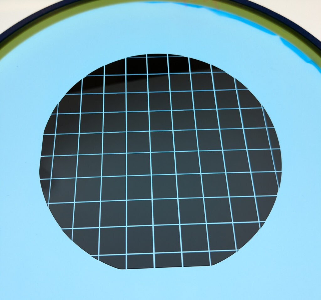
Unique Geometries
Because of the nature of stealth dicing, unique geometries such as hexagons are now possible—something impractical to do by mechanical dicing, where only continuous cuts across the substrate are generally possible. As the laser can be programmed to start and stop throughout the cut, producing arbitrary dashed lines, there are far more possibilities for design layout.
A stealth-diced 150 mm diameter Si wafer with a unique geometry only possible by stealth dicing
Want to know more?
Over the coming weeks, staff will be working to fully commission the tool to open for staff-only processing project submission; user training is not being offered on this tool at this time. Additional information on specimen compatibility can be found on the tool page. If you think that stealth dicing is a viable process to add to your fabrication workflow, please reach out to Aaron Hryciw (ahryciw@ualberta.ca) or Breanna Cherkawski (bcherkaw@ualberta.ca).
Career Opportunity - University of Windsor
The nanoFAB is pleased to post the following opportunity at University of Windsor.
Optical Profilometry Unlimited - Keyence VK-X3050 3D Surface Profiler
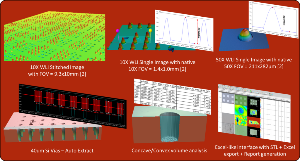
The nanoFAB is pleased to announce the installation of a multi-mode Optical Profilometer from Keyence. The Keyence VK-X3050 is a red laser scanning confocal system equipped with confocal, white light interferometry (WLI), and focus variation metrology modes. The tool natively offers wide-area scanning through stitching modes. Feature-aligned, repetitive, and correlative multi-objective multi-mode measurements are enabled through user-defined Teaching modes.
100x100mm automated stage supporting up to 4" Wafers'
Through film laser thickness measurements (>1um)
Resolution:
The three analysis modes support a scaled level of resolution and accuracy. Users can combine any of the three modes to support analysis needs down to 1nm Z-resolution in Confocal and Focus Variation modes, and 0.01nm Z-resolution in WLI mode.
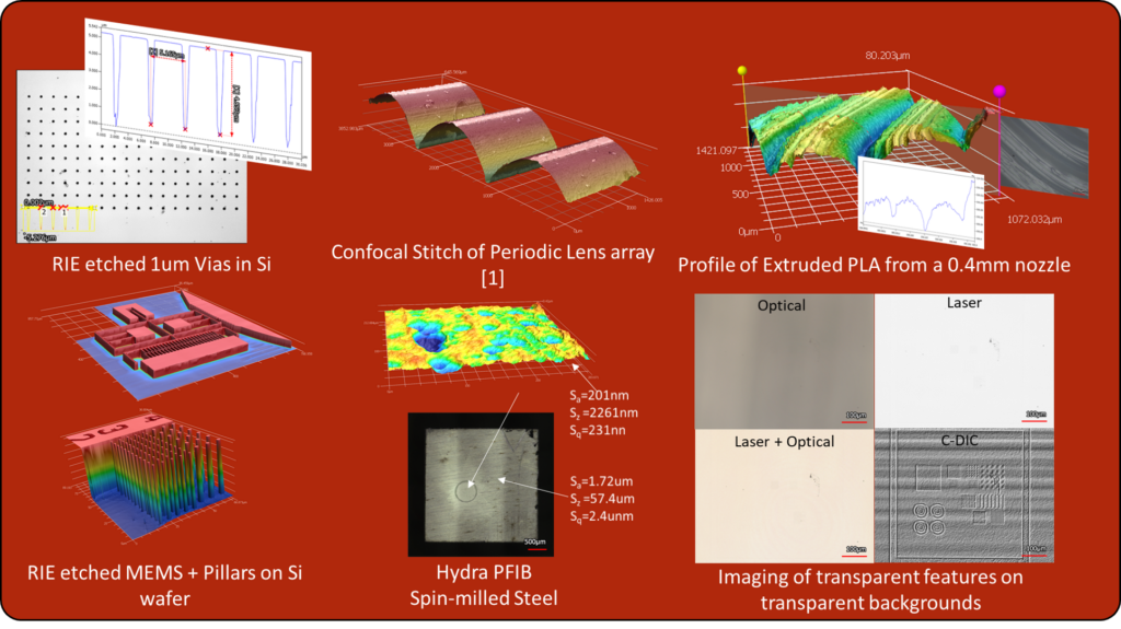
Laser Scanning Profilometry
The system is equipped with a high-resolution 16-bit photomultiplier that enables deep feature extraction of hard-to-analyze features such as 1µm Silicon vias. The system has demonstrated 30µm of depth resolution in narrow/confined grooves in some applications. Leveraging the high-resolution measurement capability, the automated XY stage (100mm x 100mm) allows for larger-scale analysis using single or multiple objectives. The automated measurement allows for stitching of large area samples with spatially separate or continuous features. Beyond the profilometry capabilities, optical observation can be supported, coupled, and enhanced by the laser observation modes, enabling transparent feature on transparent substrate imaging.
The Keyence VK-X3050 features a red laser diode and has demonstrated high performance imaging on high aspect ratio etched silicon, transparent bulk materials [1], 3D printed plastics, ion polished steels, and finding pesky transparent features on transparent substrates. [1] Lens array provided by Avalon Holographics as part of their 3D holographic display system
White Light Interferometry and Analysis software
In cases where Confocal microscopy fails to resolve features, the WLI mode acts not only as a complement but also as an enhancement. The WLI mode allows users to level samples through intelligent tip-tilt alignment with guided steps to achieve high-resolution measurements. The resulting files can be analyzed in the same browser as the laser confocal modes and are easily tracked by utilizing the built-in measurement metadata.
The Keyence system is equipped with white-light interferometry for high-resolution tasks and can measure transparent lens arrays [2] at 10/20/50X magnifications with native and ultra-wide FOVs. Dynamic software allows for automated feature measurements and volumetric analysis, and includes a user-friendly Excel-like interface for demanding tasks. [2] Optomechanical sensors arrays are provided by Kyle Scheuer from Ultracoustics Technologies LTD
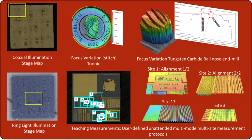
Focus variation profilometry and Teaching Modes
The system features a built-in sample mapping mode that supports any objective and allows mapping in laser and optical observation modes. Defect inspection is achievable through this feature mapping by ring-light illumination, allowing for highlighting of defect locations. The Coaxial/Ring light modes are supported by a Focus Variation Profilometry technique, enabling fast measurement of millimeter-scale features of bulk metals, coins, and machined parts. Any of the three modes, techniques, or setups can be further enhanced by the Teaching Measurement mode. Teaching Measurement modes allow for multi-mode, multi-objective, multi-site analysis that can be feature aligned across multiple runs or iterations performed today, or tomorrow.
Unique to this platform is coaxial and ring light illumination, useful for general microscopy and defect inspection. In cases of extreme feature sizes (mm scale) Focus variation techniques allow for measurement of diffusive or irregular bulk samples. The system couples these modes into an unattended automation (Teaching Mode), defined by users to allow for automatic multi-objective, multi-technique measurements at the click of a button.
Career Opportunity - Jones Microwave Inc.
The details of the positions, including responsibilities, qualifications, experience, and education are listed in the following links: