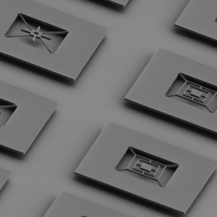
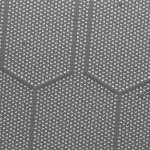
To supplement our current 30kV Electron-beam lithography (EBL) capabilities, exposure at 100 kV is now available as a service to nanoFAB academic users. In partnership with the Quantum-Nano Fabrication and Characterization Facility (QNFCF) at the University of Waterloo, we are offering this service to any academic groups who would benefit from the higher throughput, higher resolution, and improved stitching and overlay precision that is possible with a 100 kV JEOL JBX-6300FS EBL tool, as compared with our current RAITH150 Two EBL system. Only the exposure step will be performed at QNFCF: resist-coating and development are to be done at the nanoFAB by the user. This service will be charged to nanoFAB users’ projects on a cost-recovery basis.
Any nanoFAB users with academic projects may submit specimens to be exposed using the following process:
- The user submits a request on LMACS, of type EBL Service. Each distinct GDSII design to be exposed should be submitted as a separate request item within the request, and must include the following details:
- Substrate dimensions
- Substrate material(s)
- Substrate quantity (if multiple substrates are to be patterned with the same design)
- Substrate processing history (e.g., existing patterns on chip, bare substrate, etc.)
- Total number of layers to be patterned using EBL Service
- E-beam resist
- CD (smallest lateral feature size)
- GDSII design (upload file to request item)
- Layout details: GDSII cell name(s), layer, exposure coordinates. A diagram may be uploaded for clarity.
- nanoFAB staff review the submission, asking for more information if necessary.
- If the submission is approved, the user prepares the specimens for exposure (cleaning, spin-coating with resist/anti-charging layers, etc.)* and gives them to nanoFAB staff in a specimen-holder suitable for shipping (e.g., wafer carrier, gel-pak, etc.).
- nanoFAB staff prepare the GDSII data for exposure and ship the specimens to QNFCF.
- The specimens are exposed on the QNFCF JEOL JBX-6300FS system; expected turnaround is 1–2 weeks.
- Upon receiving the specimens back at the nanoFAB, the user develops the exposed resist.*
* Users may request for these steps to be performed by nanoFAB staff (tool and staff time to be charged to user’s project).
Please note that, as with any micro/nanofabrication process, multiple iterations may be necessary to achieve a desired result. All work will be performed on a best-effort basis.
For more information, please contact Aaron Hryciw (ahryciw@ualberta.ca).