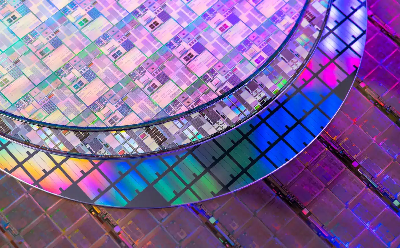
With over $110M worth of micro and nanoscale fabrication and characterization equipment and infrastructure,
Our instruments and cleanroom laboratory provide access to a wide variety of capabilities. With our dedicated staff for training and on-site technical assistance for process development and analysis, we are an unparalleled Canadian academic facility supporting research and development.


Characterization

Fabrication
Expertise
Fee For Service
Characterization
Leveraging nanoFAB staff expertise for customized characterization sample analysis.
If your needs for characterization works are low-volume, infrequent, or if training a dedicated characterization staff member is time prohibitive, nanoFAB offers a broad range of sample analysis services on a flat rate basis.
Submissions can be made online through our Laboratory Management and Access Control System, with samples mailed or dropped off on site.
This service is available to registered nanoFAB users.
Fee For Service
Fabrication
Utilizing the extensive toolset and expertise available at the nanoFAB, we offer custom nanofabrication services for both industrial and academic clients.
A fee-for-service project may be beneficial if you are interested in contract manufacturing of your prototype or proof-of-concept device, allowing you to focus on the design, integration, and application.
All projects are required to provide draft designs, which our staff can utilize to make final mask layouts. The nanoFAB does not provide design services for development of specific devices or technologies.
Resale Items
We stock a variety of commonly used items for the convenience of our user community. If you are interested in acquiring a specialty item, please ask one of our staff members and we may be able to assist in acquiring it on your behalf.
