Lithography of 2″ wafers now possible with this new vacuum chuck.
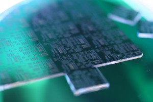
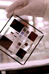
The nanoFAB has just purchased a 2″ vacuum chuck for its ABM mask aligners (MA #1,MA #2 & MA #3). This chuck will allow users to perform lithography and further processing on wafers of exotic new materials, such as GaN, Sapphire, SiC, and others. These substrates are often only available in 2″ wafer diameters. This new chuck will lead the nanoFAB into a new area of processing, that of processing devices with small feature sizes 1.5 um and larger feature sizes on exotic and costly substrates by optical lithography. The full compliment of optical photoresists can be used with this chuck. For best results, for finer features, the wafers should be at most 750 um thick. This new chuck is ready to be used and has been placed with the other custom chucks in the lithography area.

