


Ion Milling is one of the most applicable methods of sample preparation for electron microscopy analysis. While planar milling with a focused ion beam is developed and available on the Thermo Fisher Helios Hydra Plasma FIB/SEM for site specific processing, the Broad Ion Beam (BIB) system provides an automatic process to produce much larger area preparation. The Leica RES 102 BIB ion milling system at the nanoFAB, equipped with two Ar ion guns, is configured for both fast surface polishing with high energy beam and gentle polishing to produce optimum milling results for electron microscopy applications.
The RES 102 system features:
- Ion Source: Ar
- Ion energy: 0.8 to 10 keV
- Source current: Up to 4.5 mA
- Stage Rotation: 0.6 to 10 rpm
- Sample size SEM holder: max. Ø 25 mm × 12 mm
- Prepared area SEM holder: max. Ø 25 mm

RES102 BIB Ion Milling System equipped with two Ar guns
Among general electron microscopy applications, Electron Backscatter Diffraction (EBSD) is a surface technique – typical probing depth is in the range of a few tens nm for a beam energy of 20 kV. Smooth and damage-free surface is critically important to obtain high quality EBSD data. Compared to conventional mechanical polishing techniques, which can result in very rough surfaces and a thick damaged layer, low energy beam at grazing incident angle and rotating stage on the RES102 can effectively polish the surface to reduce roughness and remove the damaged layer.
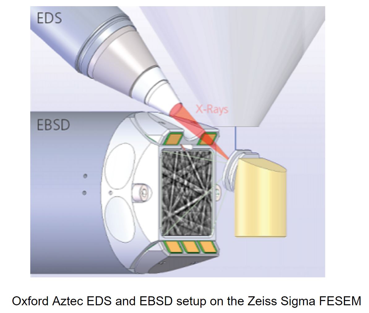
Oxford Aztec EDS and EBSD setup on the Zeiss Sigma FESEM
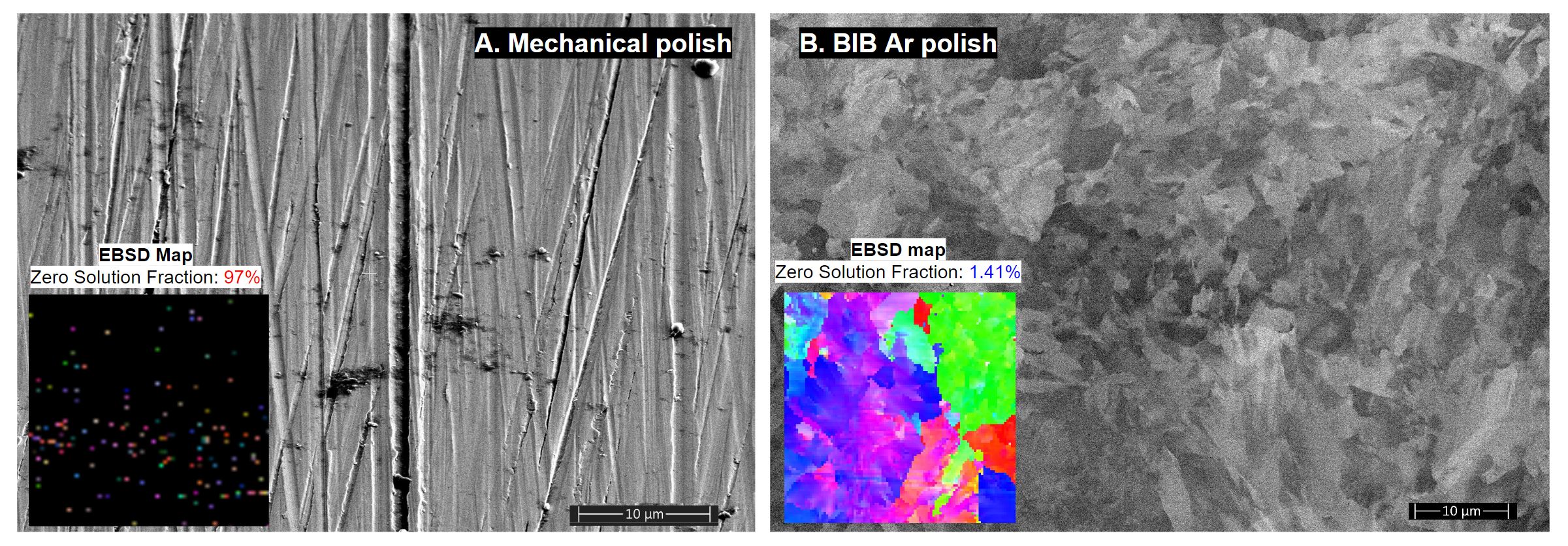
Plan-view SEM images and EBSD maps of a steel sample after (A) mechanical polish and (B) BIB Ar polish
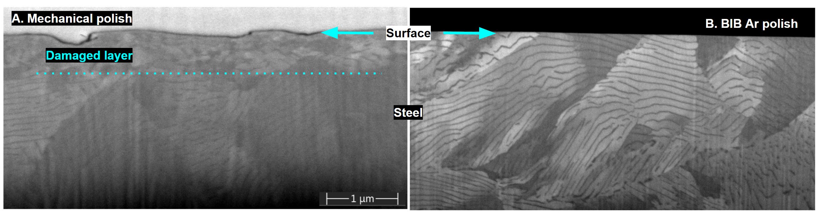
Cross sectional SEM images of a steel sample after (A) mechanical polish and (B) BIB Ar polish
With the programmable recipes of flexible parameters (beam energy, beam current, incident angle, stage rotating speed), the RES102 BIB has produced very nice results for our users for EBSD analysis. See recent examples below.
Application Examples (EBSD)
- Sample: 3D printed Alumina for structural applications
- Sample Courtesy: Cass (Haoyang) Li, Dr. James Hogan, Mechanical Engineering Department, Faculty of Engineering, University of Alberta
- Ion Milling process:
- 8 kV, 3 mA, 3.5 degrees, 1.5 rmp for 120 mins
- 8 kV, 2 mA, 2.5 degrees, 1.5 rmp for 60 mins
- EBSD mapping: 175 µm x 175 µm, stepsize 50 nm
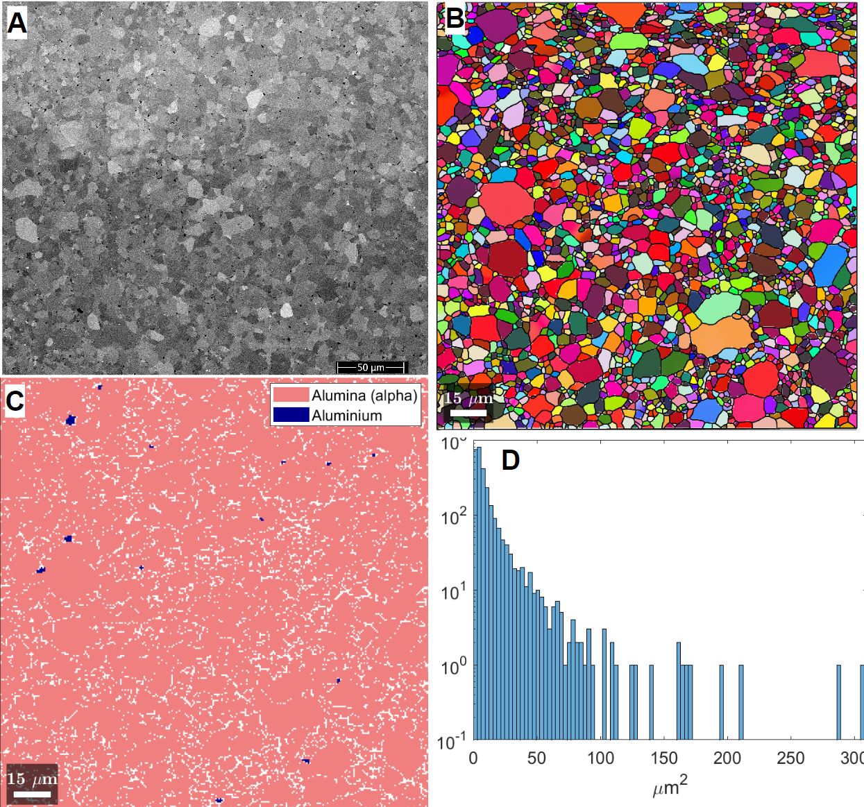
(A) SEM image; (B) Orientation map; (C) Phase maps of Alumina and Aluminium; (D) Grain size distribution
- Sample: Rail Steel
- Sample Courtesy: Stephen Okocha, Drs. Ben Jar and Michael Hendry, Mechanical Engineering Department, Civil and Environmental Engineering Department, Faculty of Engineering, University of Alberta
- Ion Milling process:
- 8 kV, 3 mA, 2.5 degrees, 1.5 rmp for 60 mins
- 6 kV, 2 mA, 2.5 degrees, 1.5 rmp for 60 mins
- EBSD mapping: 300 µm x 300 µm, stepsize 250 nm
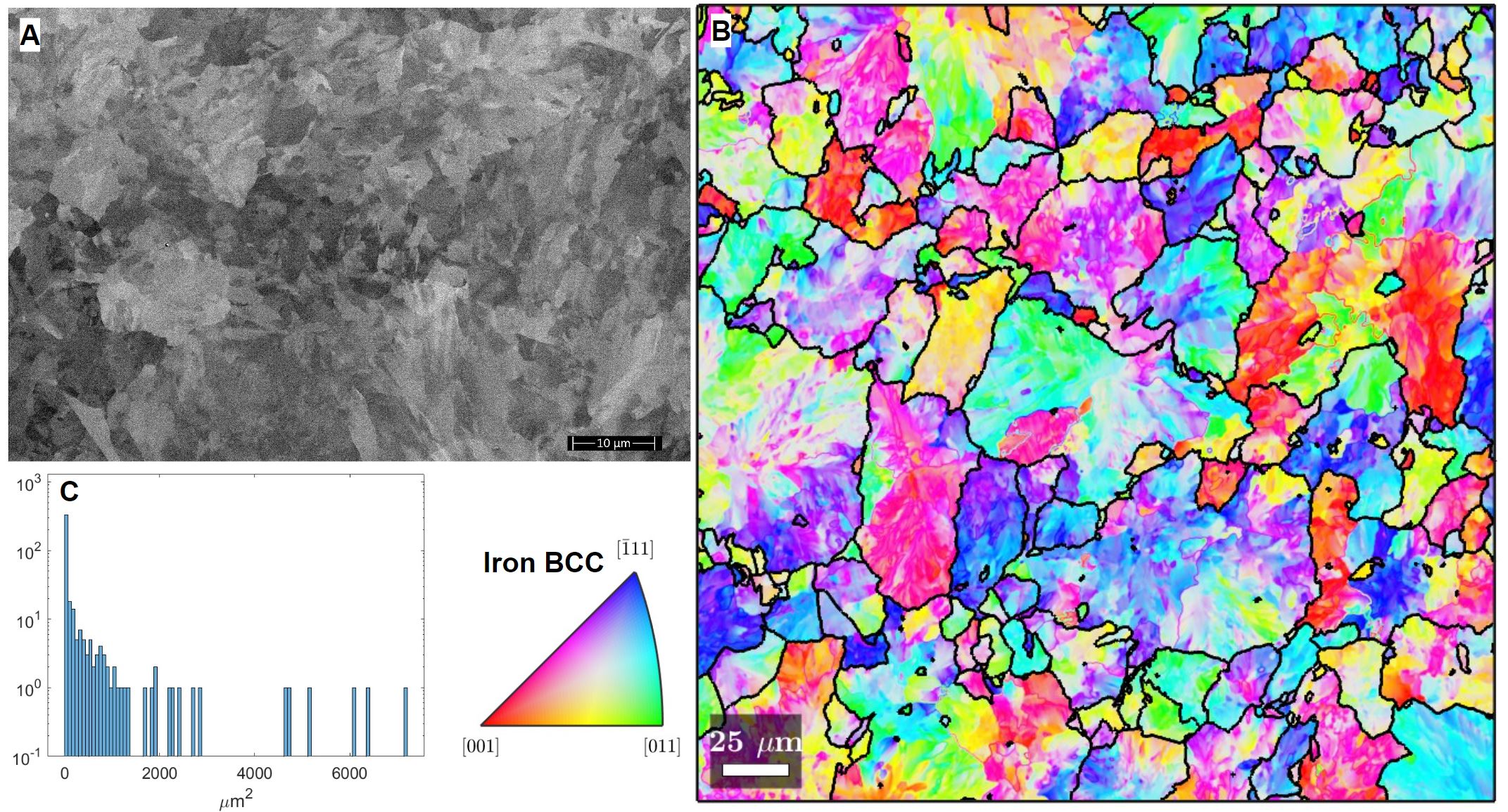
(A) SEM image; (B) Orientation map; (C) Grain size distribution
- Sample: Al-Cr-Fe-Ni medium-entropy alloy (MEA)
- Sample Courtesy: Guijiang Diao, Dr. Dongyang Li, Chemical and Materials Engineering Department, Faculty of Engineering, University of Alberta
- Ion Milling process:
- 8 kV, 3 mA, 3.5 degrees, 1.5 rmp for 60 mins
- 5 kV, 2 mA, 2.5 degrees, 1.5 rmp for 60 mins
- EBSD mapping: 2500 µm x 1500 µm, stepsize 500 nm
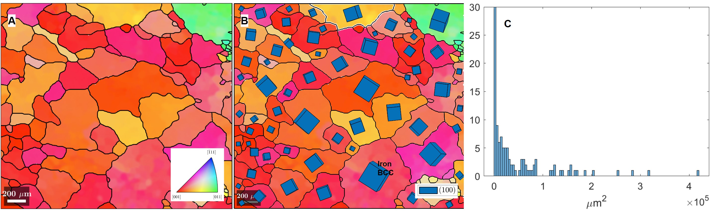
(A) Orientation map; (B) Crystal unit cell orientation and (C) Grain Size Distribution
The RES102 ion milling system is now available to general users for both staff analysis and user training. Any users interested in getting trained on this tool or staff analysis should submit a request on LMACS. If you have any questions, please contact the tool managers Drs. Nas Yousefi and Shihong Xu or Peng Li – the Characterization Group Manager.