The nanoFAB is pleased to announce that the newly installed Leica Ar Ion Milling System is commissioned and available for general user access.
The Leica EM RES102 Ion Beam Milling System is equipped with two saddlefield Ar ion sources with variable ion energy for optimum milling results. Flexible ion incidence with respect to the sample surface and broad ion beams with both high-energy milling and gentle polishing make the RES102 a unique system for both SEM and TEM microscopy application:
- Large area SEM samples – both Cross-Section and Plan-View
- High quality TEM samples for Atomic Resolution S/TEM analysis
- Gentle polishing Ga-FIB prepared lamella
A procedure of SEM sample polishing is fully developed for both cross section and plan view samples. It is available for user training now. Please submit a training request on LMACS, if you are interested to get trained on the tool. TEM sample preparation is still under development. Please contact Peng Li (Peng.Li@ualberta.ca) – the Characterization Group Manager, if you like to test or prepare your TEM samples during the recipe development or if you have any questions about TEM/SEM sample preparation.
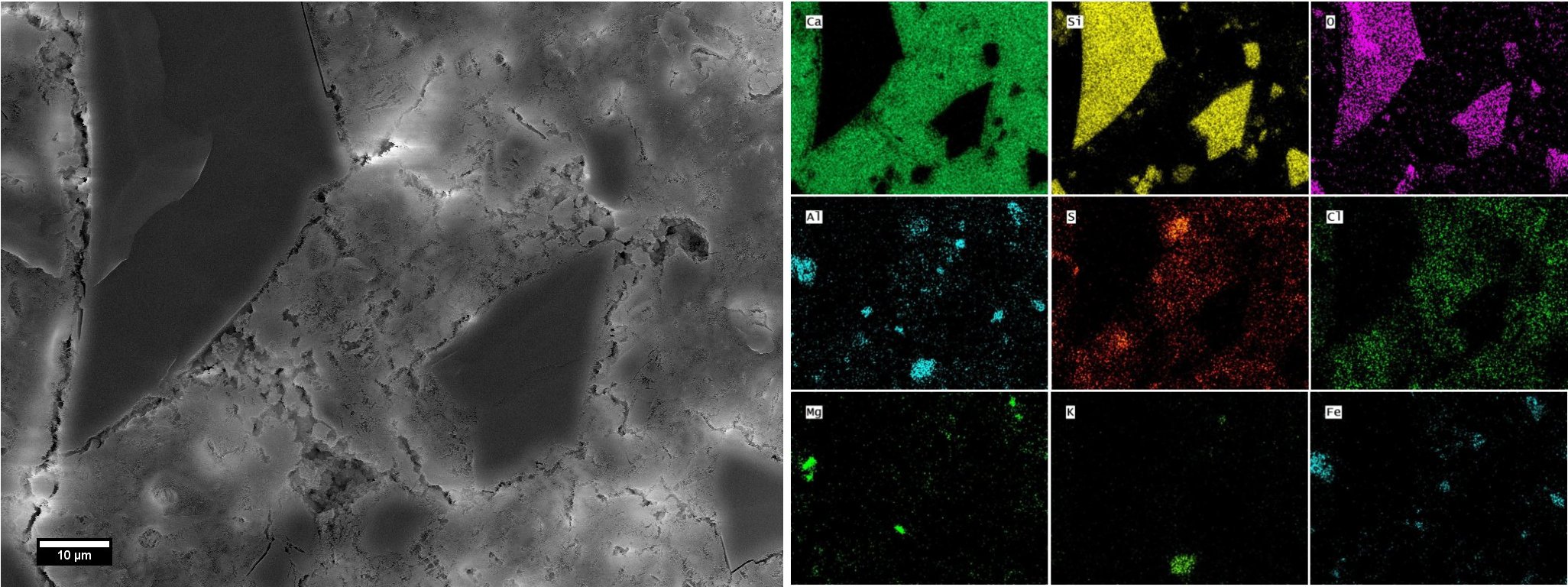
Below are some examples of polished shale, cement and microchip samples for SEM/HiM microscopy.
- Cross section of an Intel Core i7 processor
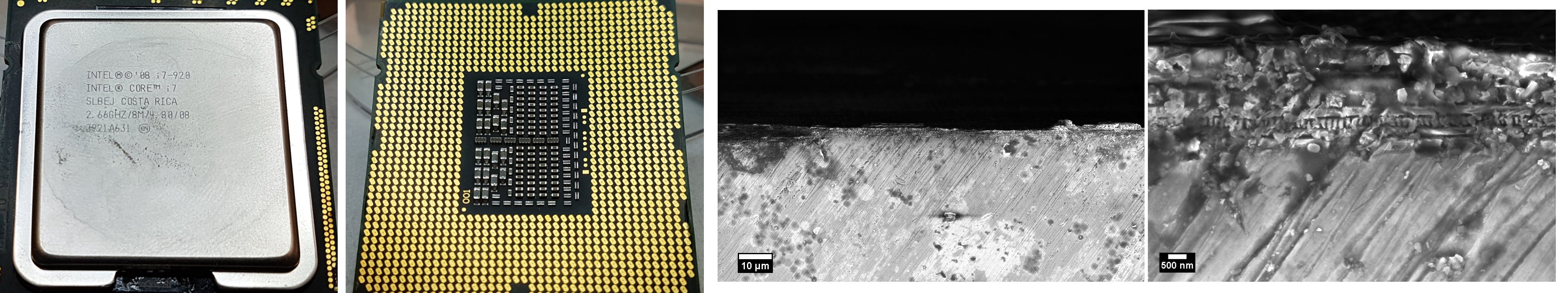
Cross section before Ion Milling (SEM images)
Cross section after Ion Milling (SEM images)
Cross section after Ion Milling (EDX Elemental Mapping)
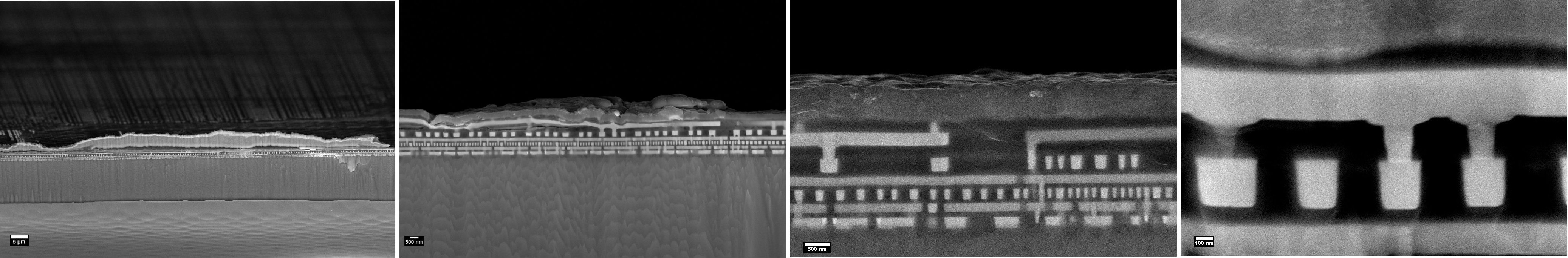
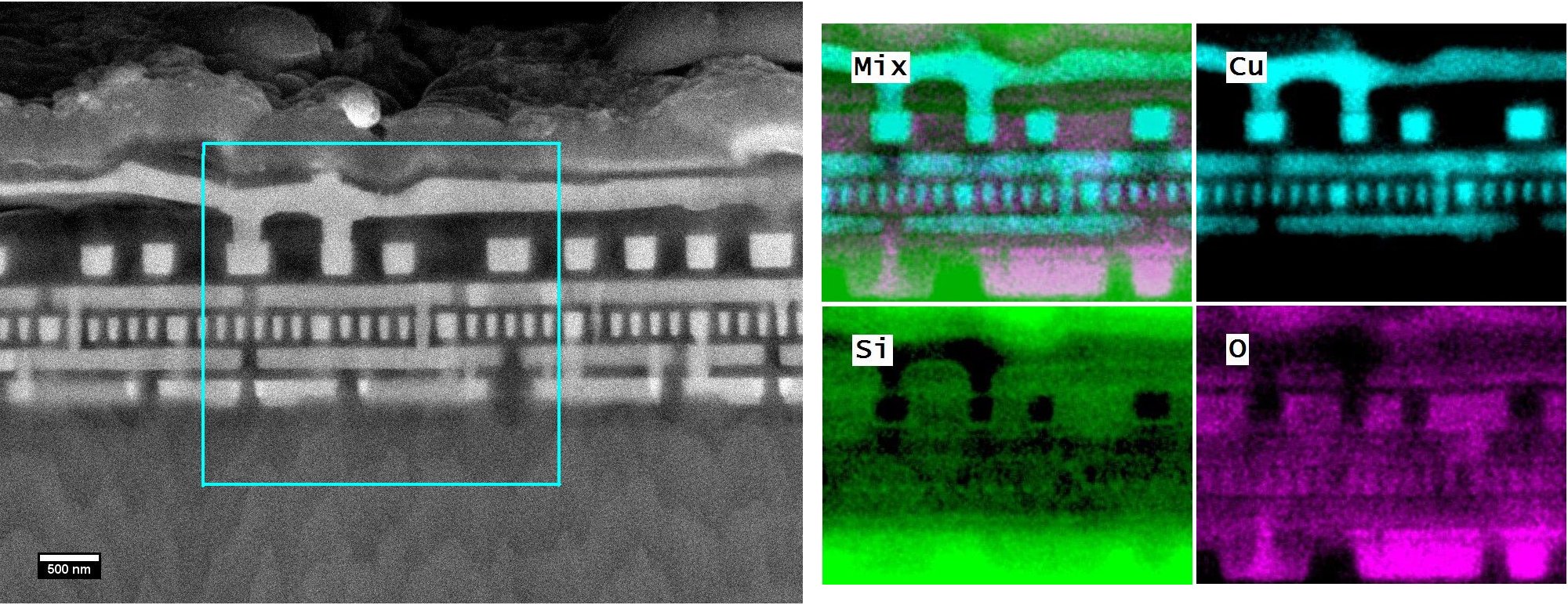
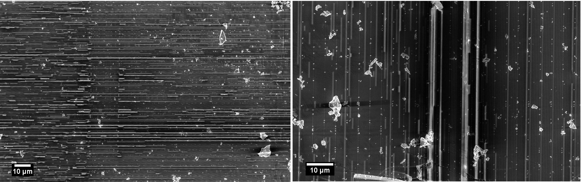
- Plan view of an Intel Core i7 processor
Plan view before Ion Milling (SEM images)
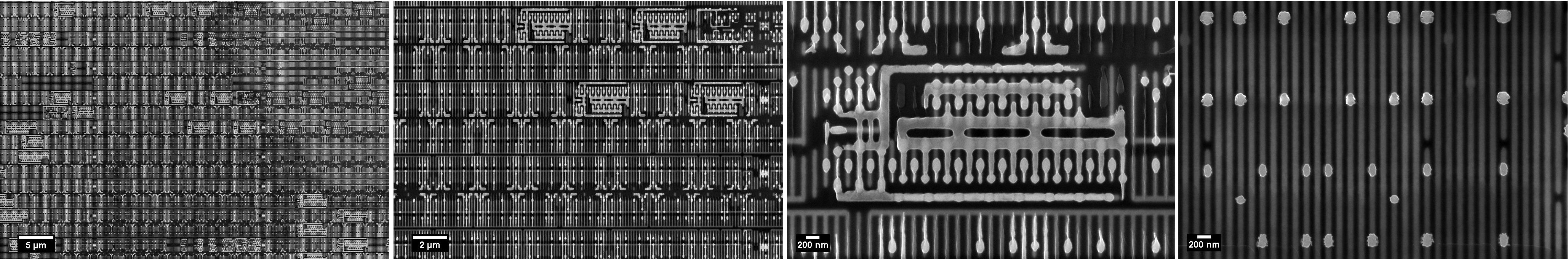
Plan view after Ion Milling (SEM images)
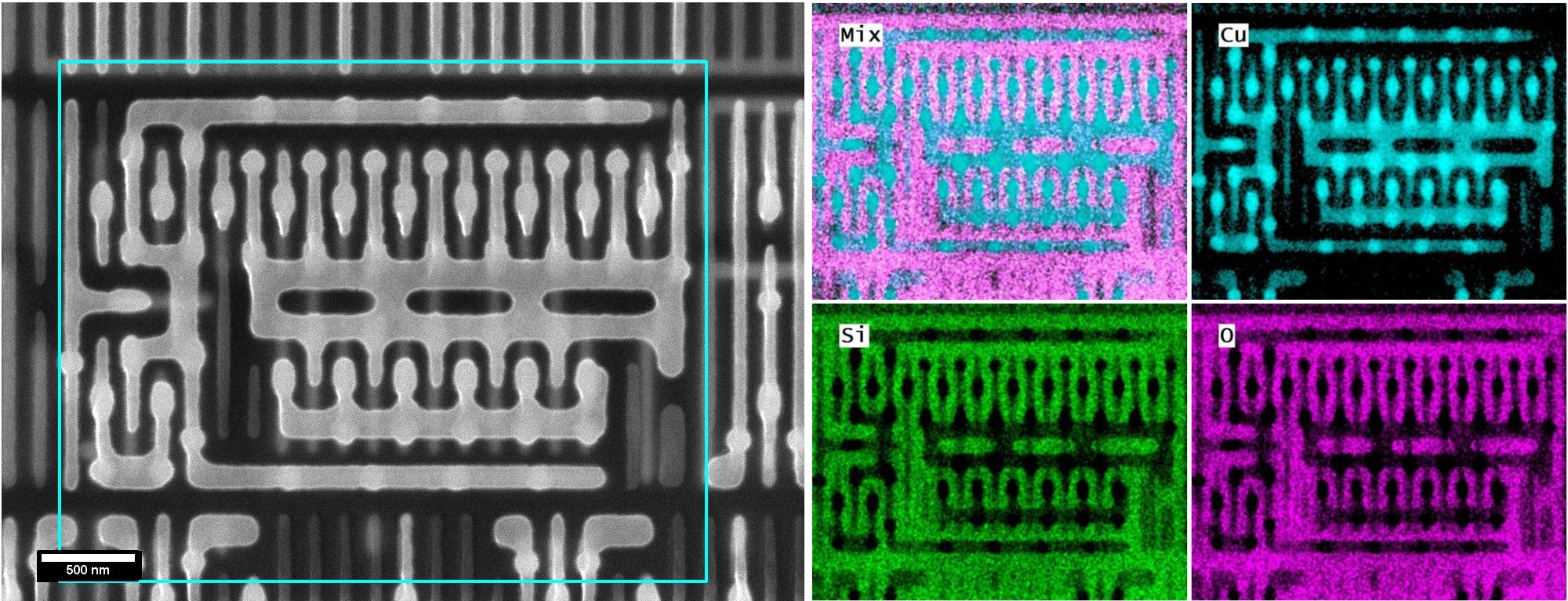
Plan view after Ion Milling (EDX Elemental Mapping)
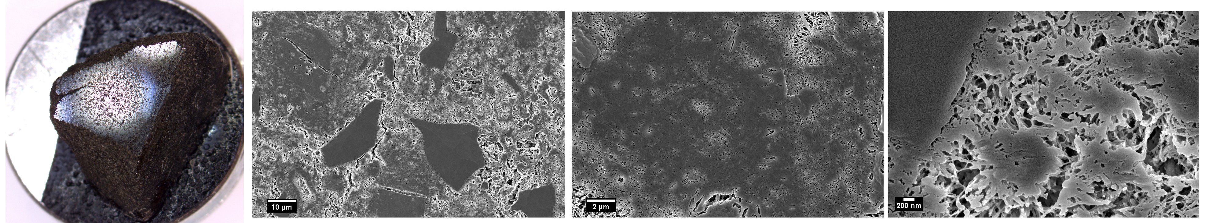
- Shale
Before Ion Milling (SEM images)
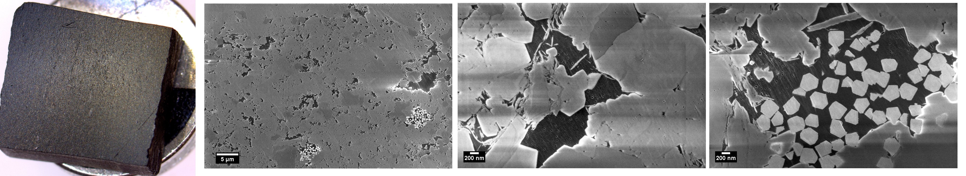
After Ion Milling (SEM images, charging effects are noticeable with native surface)
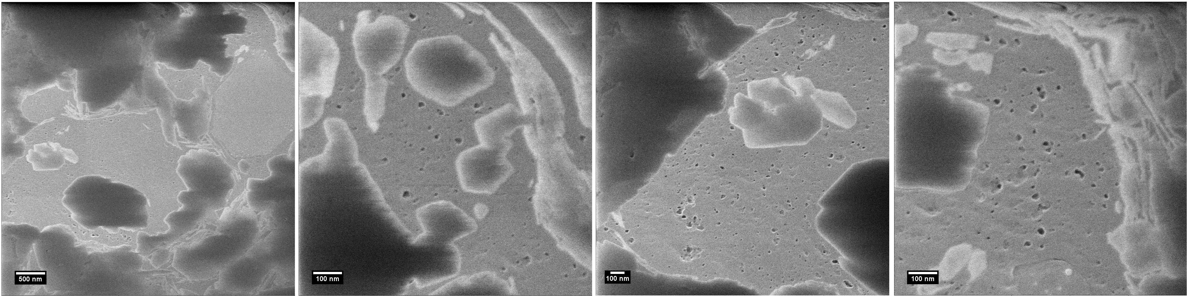
After Ion Milling (Helium Ion Microscopy, no charging effects with native surface)
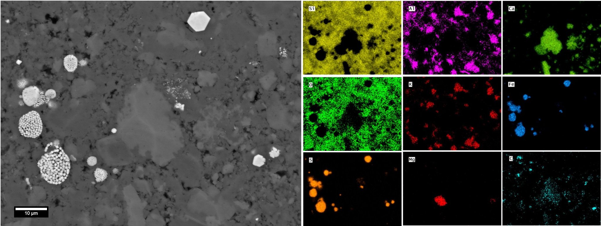
After Ion Milling (EDX Elemental Mapping)
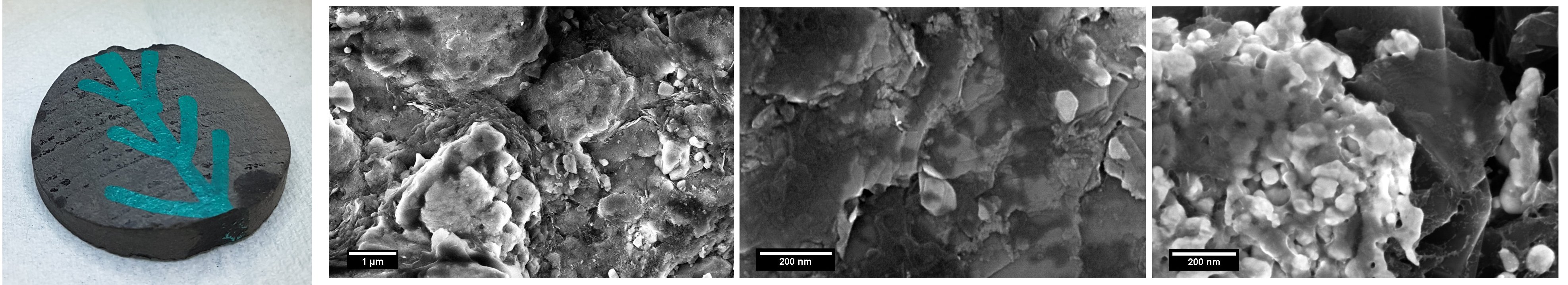
- Cement
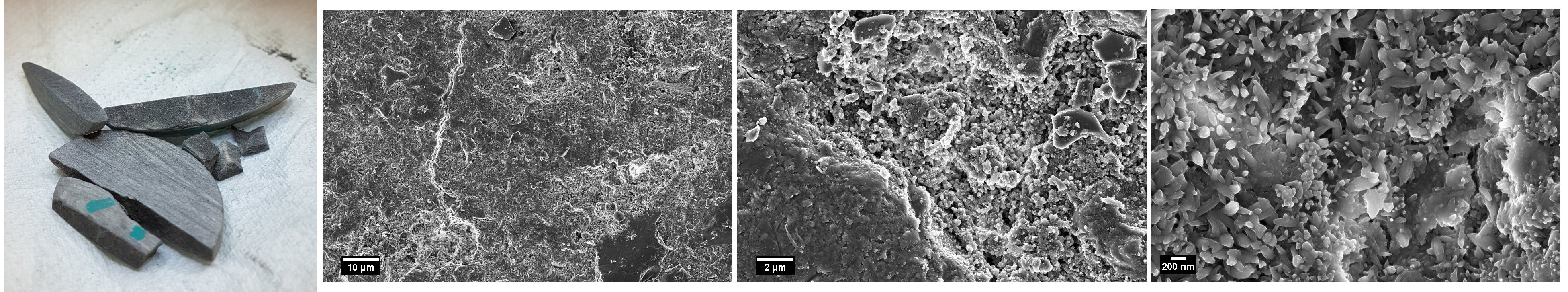
Before Ion Milling (SEM images)
After Ion Milling (SEM images)