The nanoFAB is pleased to announce that the installation and qualification of the new PHI VersaProbe III Scanning XPS Microprobe has been successfully completed.
Main features of the system include:
- Imaging/mapping capability with spatial resolution of less than 10 µm
- Depth profile analysis of both organic and inorganic materials
- Low Energy Inverse Photoemission Spectroscopy (LEIPS)
- Angle-resolved XPS
- Hot/cold stage providing temperatures of −140 °C to +600 °C
You can watch the installation of the tool at the following time-lapse virtual tour:
Trial XPS analyses will be available during the commissioning period; if you are interested in having your specimens analysed using any of the advanced capabilities on this system, please contact the Characterization Group Manager, Peng Li (Peng.Li@ualberta.ca). The system is expected to be available for user training and fee-for-service specimen analysis by Spring/Summer 2020.
Below are some testing results from tool qualification:
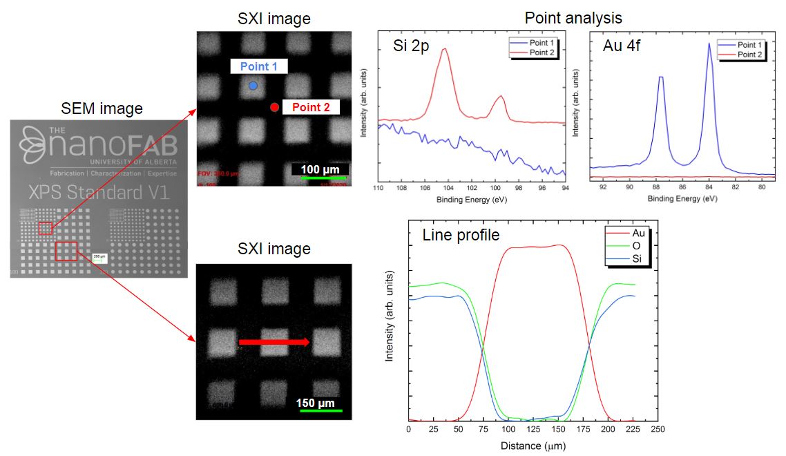
- Point / lineprofile analysis
Sample: Patterned Au film on Si substrate
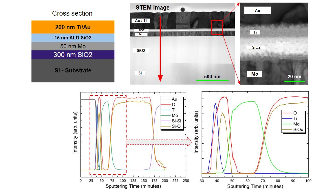
- Depth profile analysis
Sample: Multi-layer films
Sputter gun: mono-Ar
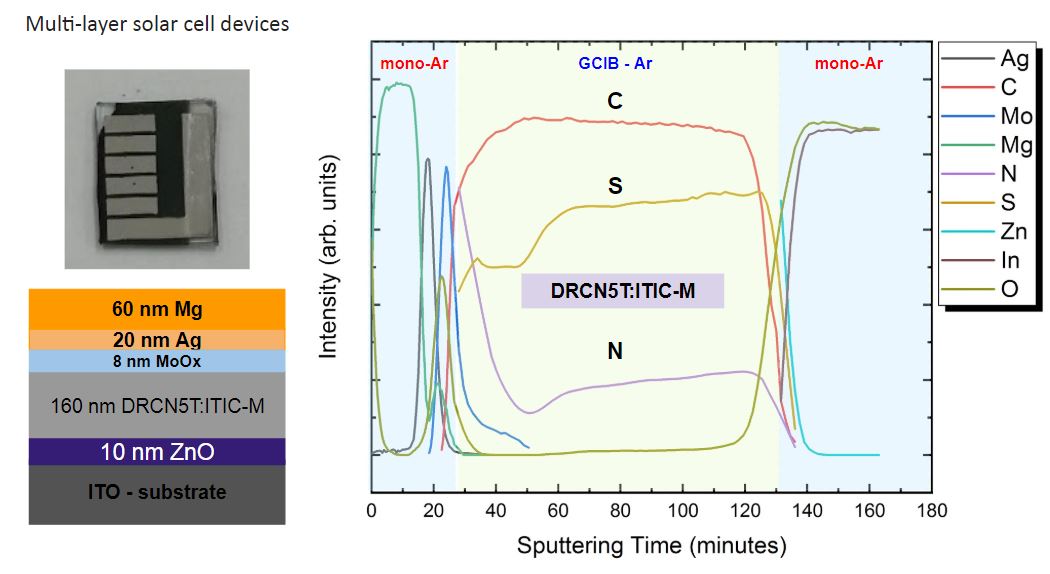
- Depth profile analysis
Sample: Multi-layer Solar Cell Device
Sputter gun: mono-Ar and GCIB
Group: Prof. Jillian Buriak, Chemistry, University of Alberta