


Last week, the nanoFAB bid the Filmetrics Resist and Dielectric Thickness Mapping System a fond farewell after more than fifteen years of dedicated service in the cleanroom. In its place, we are pleased to announce the installation of an upgraded thin-film measurement tool: a Filmetrics F50-UV.

The new F50-UV system is equipped with a dual light source: in addition to the standard tungsten-halogen lamp, a deuterium lamp may optionally be turned on to provide UV illumination in the λ ≤ 350 nm range. This extended illumination, along with a 190–1100 nm spectrometer range, enables accurate measurement of dielectric films as thin as ~5 nm.
The fast, automated stage with vacuum chuck provides an efficient means of acquiring thickness maps for specimens up to 200 mm in diameter, with both 2D and 3D visualisation of measurement results.
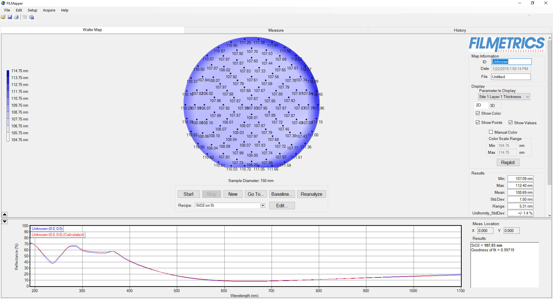
115-point thickness map of ~100 nm PECVD SiO₂ on a 150 mm Si wafer
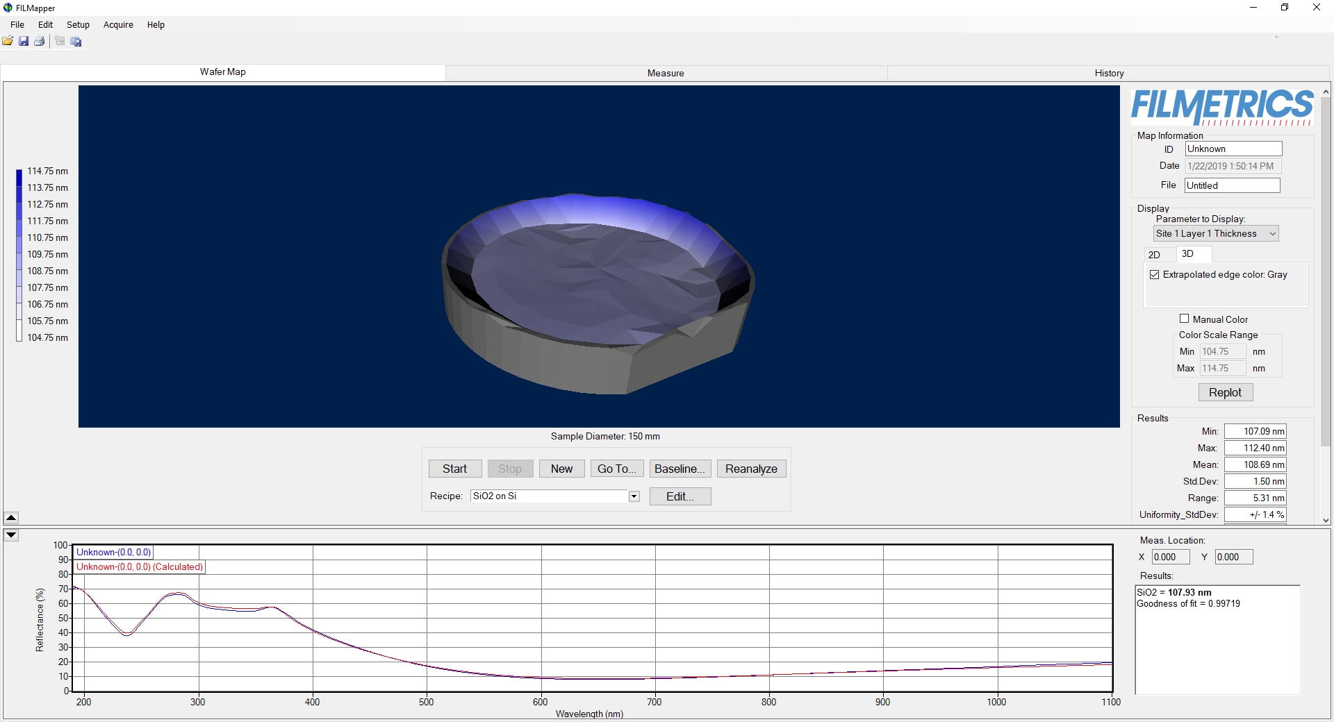
3D visualisation of previous map
The Filmetrics F50-UV is now available for user training—please submit a training request on LMACS if you wish to use this tool.
Features
- Substrate size: ~5 mm × 5 mm to 200 mm diameter
- Thickness measurement range: 5 nm – 40 µm
- Min. thickness to measure n and k: 50 nm
- Wavelength range: 190–1100 nm
- Spot size: 1.5 mm
- Light source: deuterium + tungsten-halogen (dual light source: may choose one or both lamps)
- Measurement results visualisation in 2D and 3D