The newly installed JEOL JEM-ARM200CF Atomic Resolution S/TEM is fully commissioned, and now open to general users. This probe aberration corrected S/TEM features high resolution TEM/STEM imaging and fast EDX chemical mapping, which enables researchers to explore the atomic structure, morphology and chemical composition of materials at the sub-nanometer scale. Detailed specs of the microscope can be found in the previous facility news.
Like all other tools at the nanoFAB, users can access to the TEM analysis by both user training/self-use and staff analysis. Training pre-requisites include sufficient TEM background and hands on experiences. Sample and analysis details are required prior to scheduling sessions for sample analysis by staff. In either case, submit a request on LMACS and you will be contacted by our TEM staff. If you have any question, please contact Peng Li (Peng.Li@ualberta.ca) – the Characterization Group Manager,
Below are some example STEM/EDX mapping results from our user work:
- Sample: Pd/Pt nanoparticles
User/Group: Hanieh Nassiri / Prof. Natalia Semagina, CME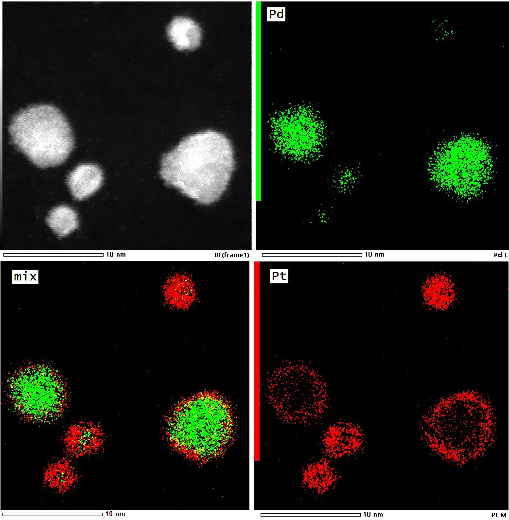
- Sample: Ce/Co/Ni/Zr nanoparticles
Uer/Group: Dr. Jing Shen / Prof. Natalia Semagina, CME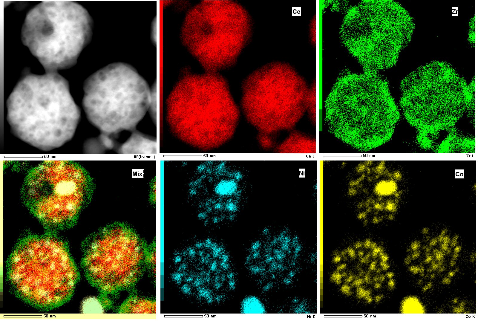
- Sample: Pd/Pt nanoparticles encapsulated in SiO2
User/Group: Amir Hossein Habibi / Prof. Natalia Semagina, CME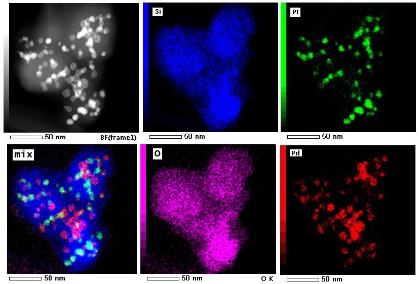
- Sample: Cross section of ZnO2 coated nanostructured ITO
User/Group: Dr. Bing Cao / Prof. Jillian Buriak, Chemistry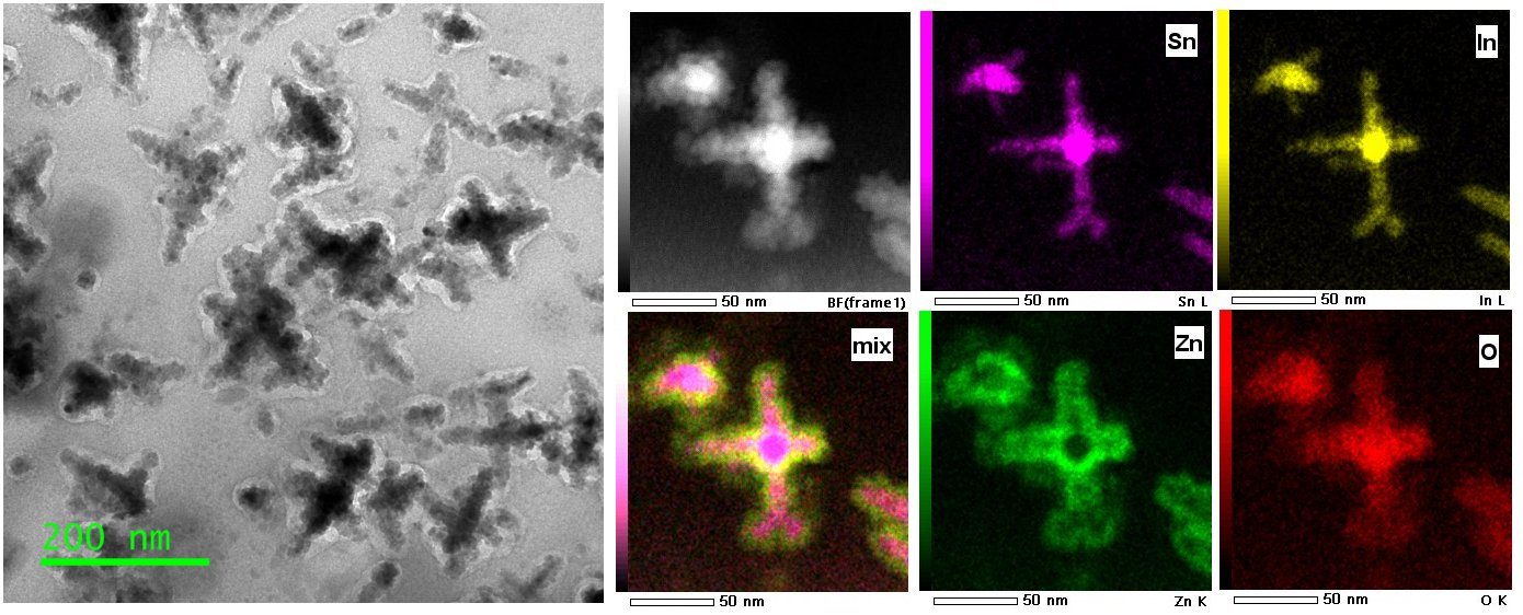
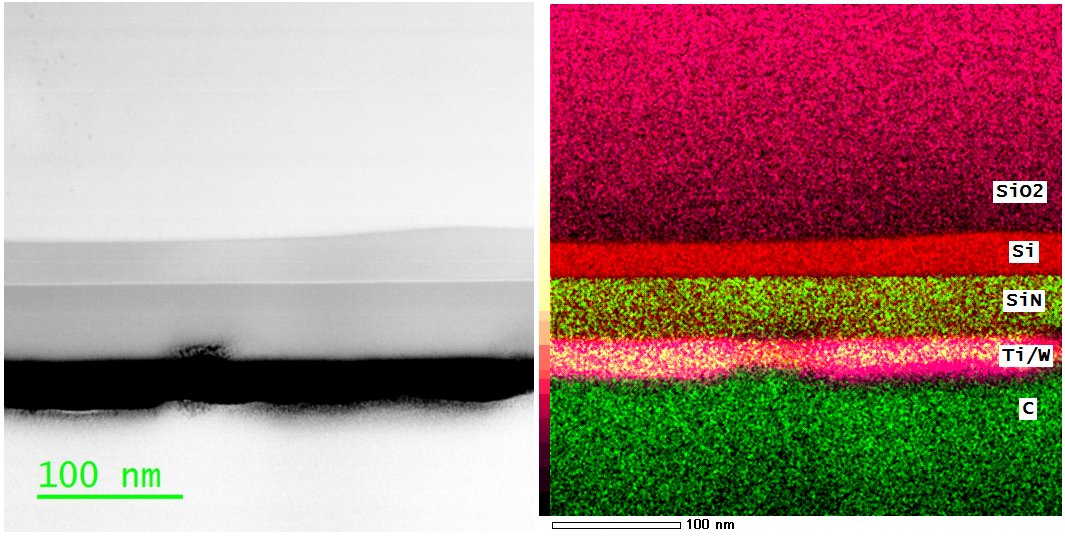
- Sample: Cross-section of a multi-layer MEMS device
User/Group: Mojtaba Safari, Hooman Hosseinkhannazer / Norcada Inc.