


The ExactaCoat, an ultrasonic spray coating system, can accommodate specimens up to 300 mm in diameter. This tool is primarily used for photoresist coating in situations where conventional spin coating is impractical or yields poor results: specimens that are too fragile, exhibit large topographical variations, or possess irregular shapes.
The spray coater offers a particular advantage for specimens where topography presents a challenge to achieving good film uniformity during spin coating: examples include MEMS or microfluidic devices with deep (tens to hundreds of µm) features etched via DRIE or KOH/TMAH. Process development is currently underway to formulate recipes suitable for coating deep and/or high aspect ratio topography wafers. Additionally, spray coating is a valuable technique for those looking to apply photoresist as a dicing protect layer on extremely fragile or through-etched substrates that are not compatible with spin coating.
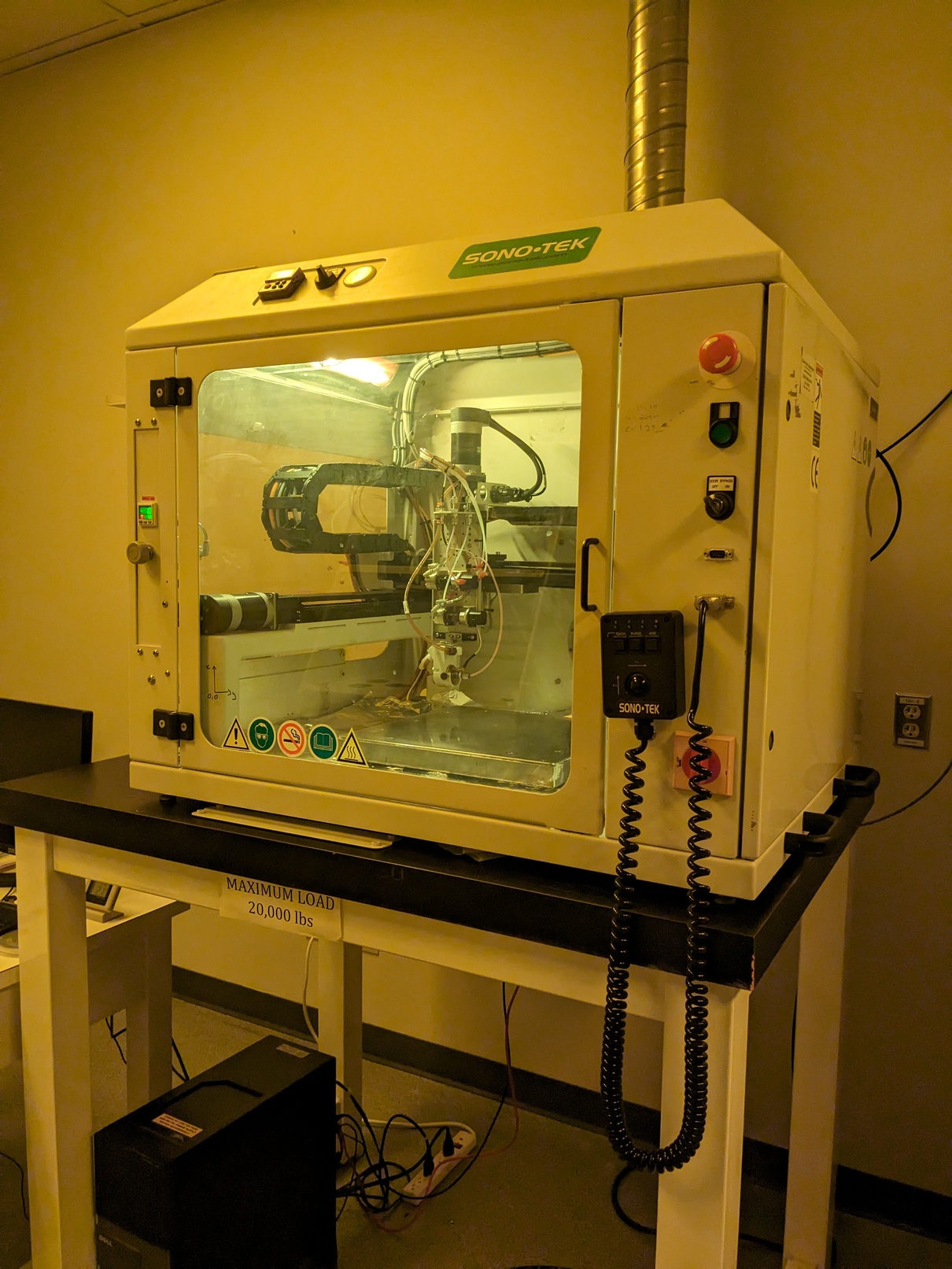 The Sono-Tek ExactaCoat Spray Coater
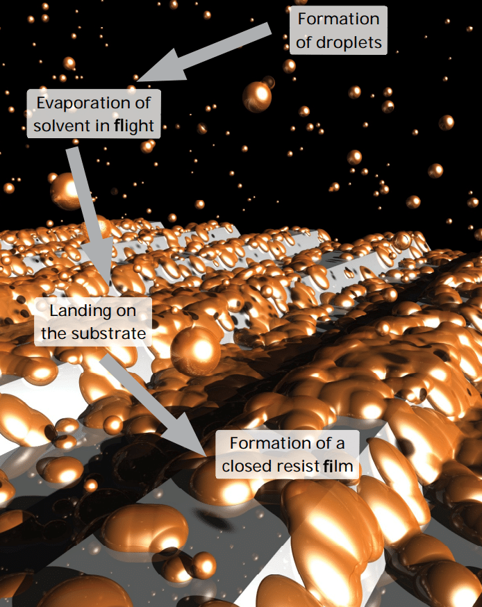 Schematic of the spray coating process (MicroChemicals)
To coat an extended specimen such as a wafer, the spray of atomised resist is rastered across the work area in overlapping stripes. This is illustrated in the following videos, where a cleanroom wipe is used to show the sprayed resist more clearly.
After spray coating a wafer with resist and softbaking, it may be exposed and developed to complete a photolithography process. The following optical microscope images illustrate some preliminary results of photolithography on Si wafers, showcasing excellent film uniformity and achieving lateral feature sizes as small as 5 µm.
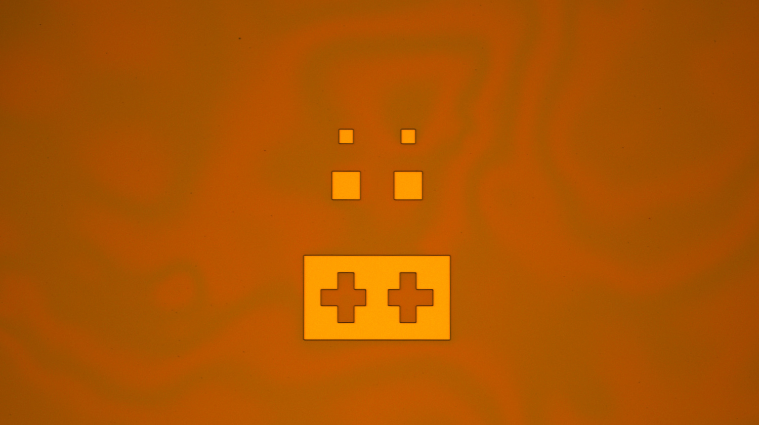
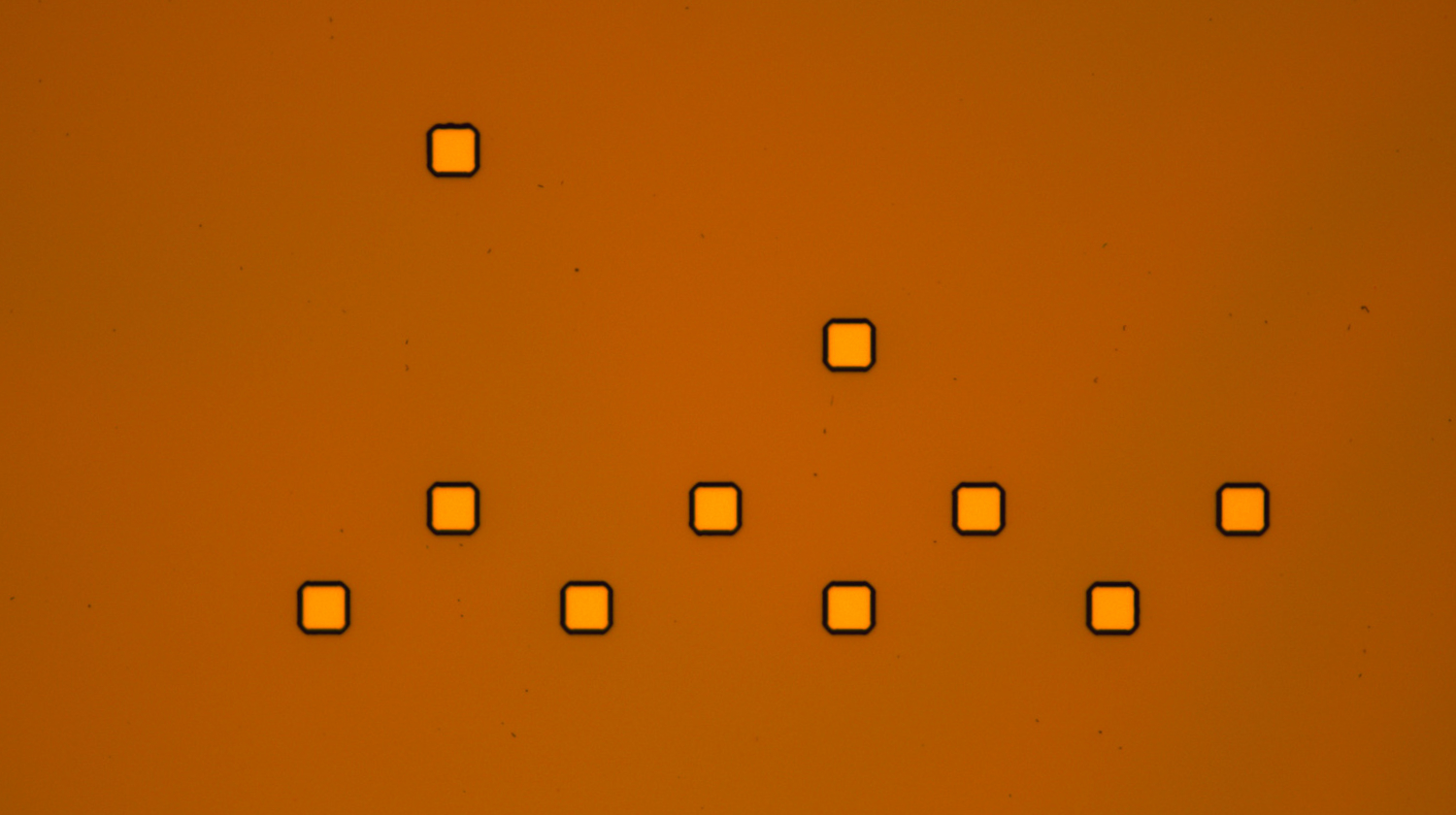
Photolithography using spray coating: Si wafers spray coated with a ~4.5 µm thick film of AZ 1505, exposed in a contact mask aligner, and developed. The smallest feature size pictured in each image is 5 µm.
We are thrilled to introduce this new capability, along with the array of associated applications it makes possible. If spray coating is a technique you feel would be beneficial to your work, please submit a request through LMACS to receive training. If you have any questions, please do not hesitate to contact Breanna Cherkawski or Aaron Hryciw.
Resources
- Application note: Spray coating (MicroChemicals GmbH)