


Bonding techniques include:
- Anodic (borosilicate glass to Si)
- Direct (Si to Si)
- Eutectic (Si to Si or Si to glass with intermediate metal layer)
- Thermocompression (bonding between metal films deposited on both substrates)
- Other custom bonding techniques
Technical features:
- Up to 150 mm wafer sizes (100 mm and 150 mm hardware available)
- In situ alignment (visible and IR) with 1 µm accuracy; manual and automatic (image recognition) alignment procedures available
- High vacuum (10-6 Torr)
- Wafer separation of 30 mm
- Independent platen temperature control, up to 560 °C
- Radical activation (RAD) for in situ surface cleaning and activation
- Bonding forces up to 40 kN
- Anodic bonding voltages up to 2.5 kV, current limits up to 8 mA
- Triple-stack anodic bonding
- Wafer edge clamping (no contact on bonding surfaces)
Application Examples
Anodic Bond: borosilicate glass to Si
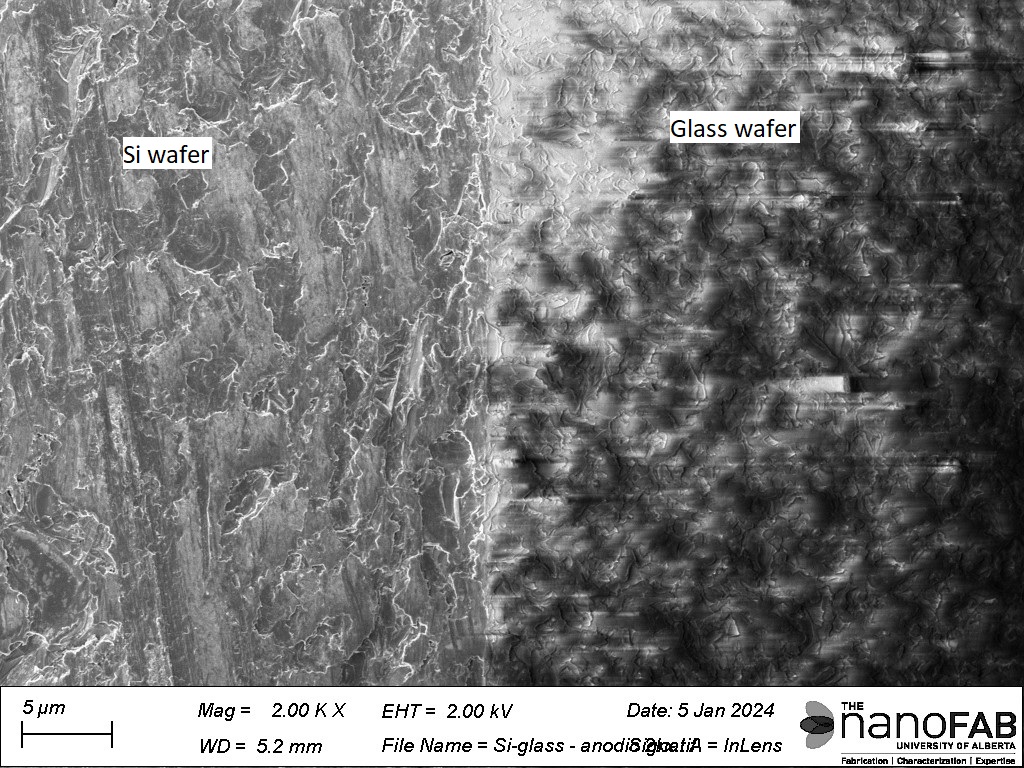
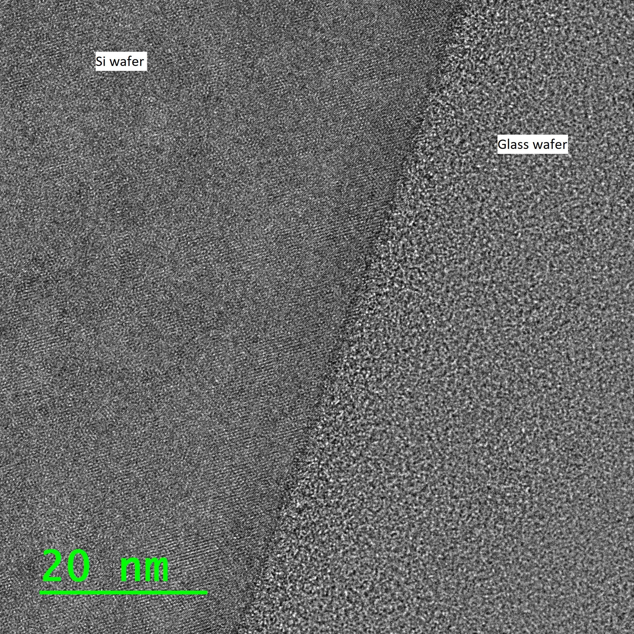
Cross-sectional SEM (left) and TEM (right) images of bonding interface.
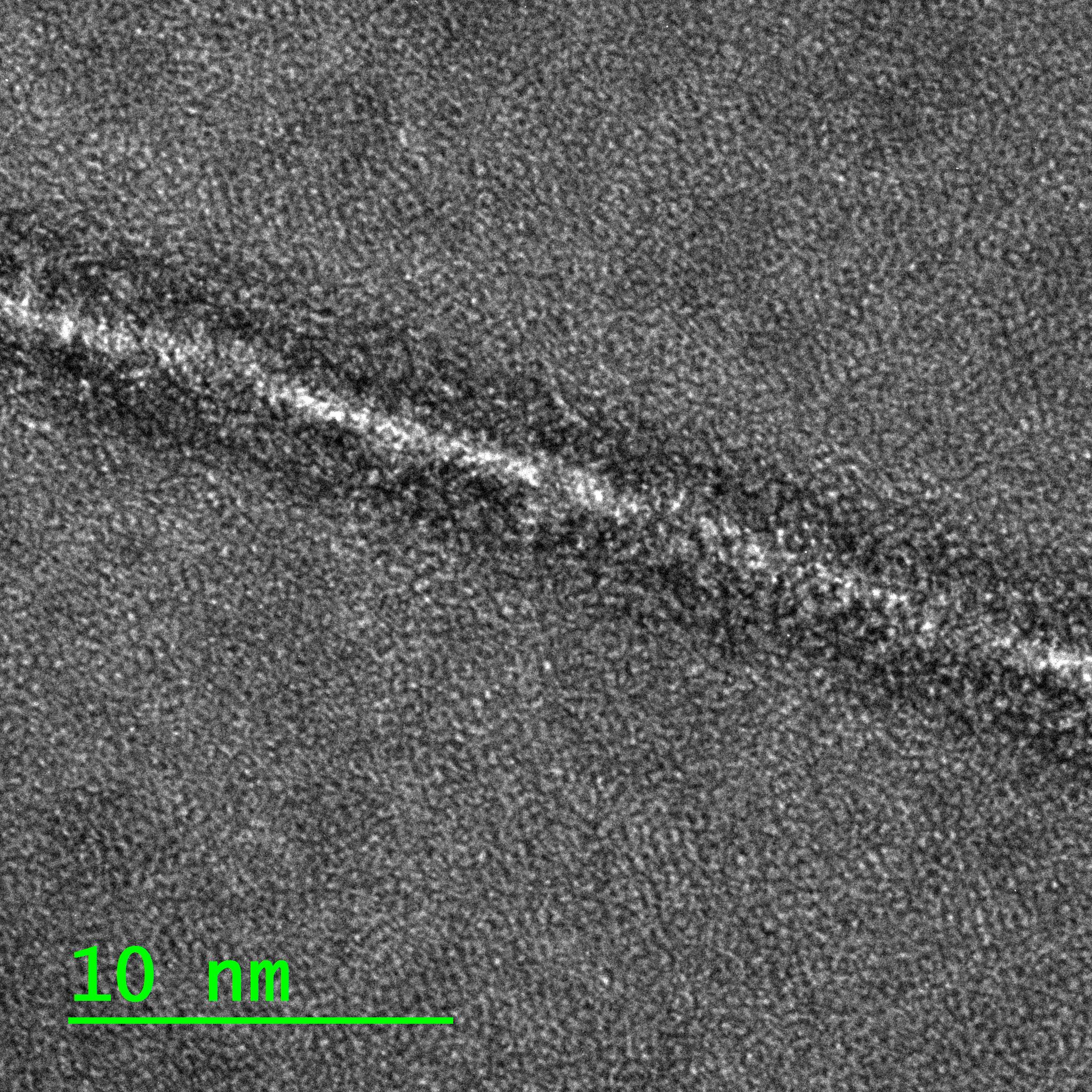
Si–Si Direct Bond: in situ RAD + low-temperature anneal
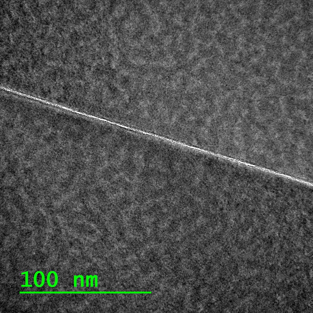
TEM images of the bonding interfaces of silicon wafers after a low-temperature (250 °C) anneal performed in the AWB-04 chamber without breaking vacuum. The thin amorphous native SiO2 layer can be seen along the interface.
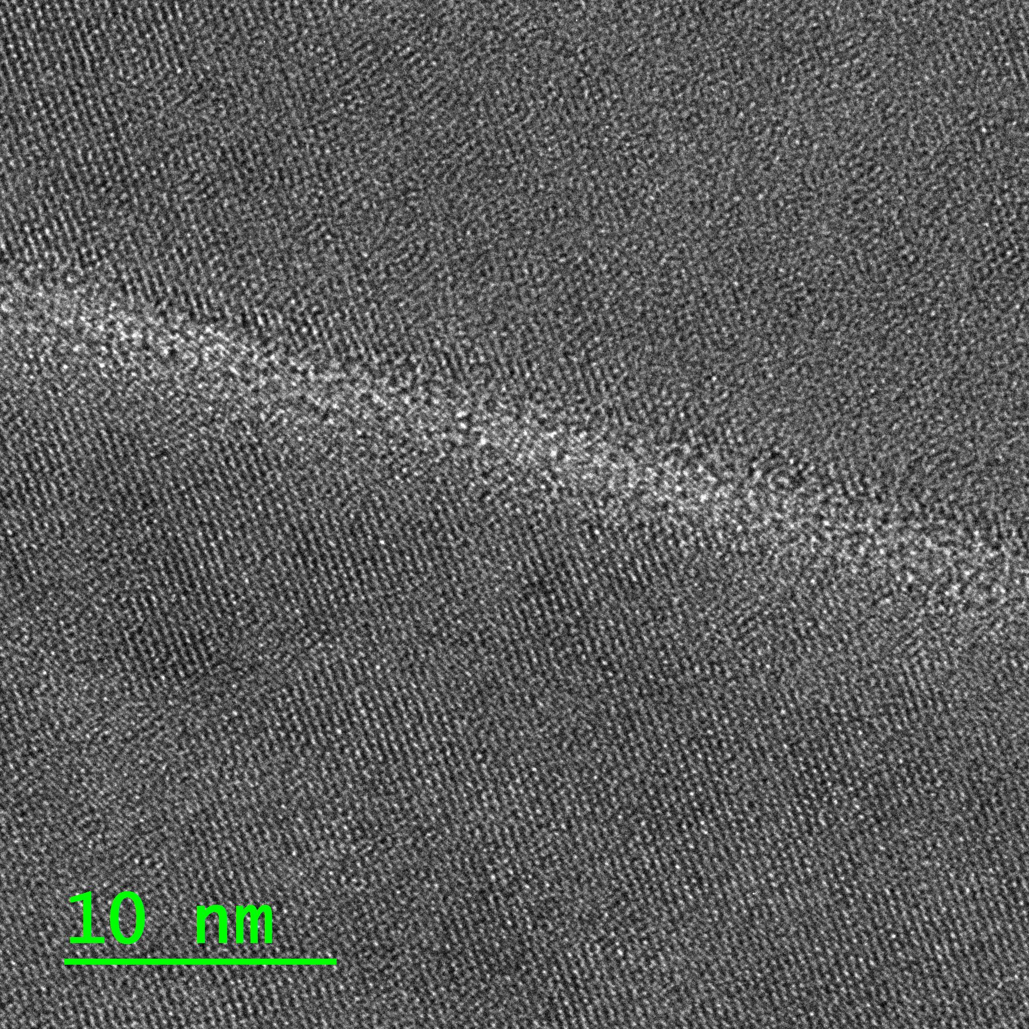
Si–Si Direct Bond: in situ RAD + external high-temperature anneal
TEM images of the bonding interfaces of silicon wafers after a high-temperature (1100 °C) anneal performed in Tystar General Anneal (Tube 6). The thin amorphous native SiO2 layer can be seen along the interface, but has diffused into the bulk Si layer.
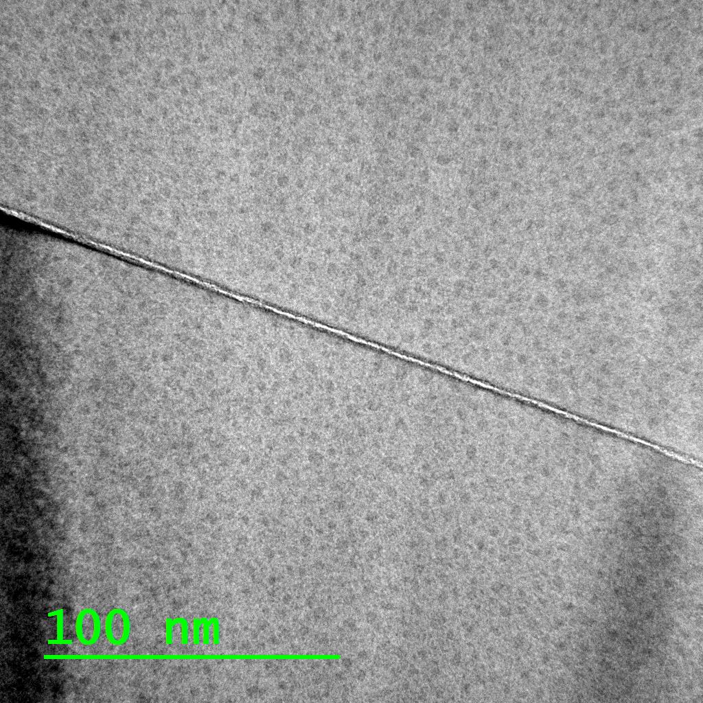
Au–Au Thermocompression Bond: Si to Si with Au interlayers


SEM images of silicon wafers bonded via Au–Au thermocompression bonding: full wafer cross-section (left) and close-up of bond interface (right). Patterned Au films are deposited on Si wafers and bonded using moderate temperatures (~300 °C) and high pressures (~7.5 MPa). Images courtesy of Jones Microwave Inc. and RM3.
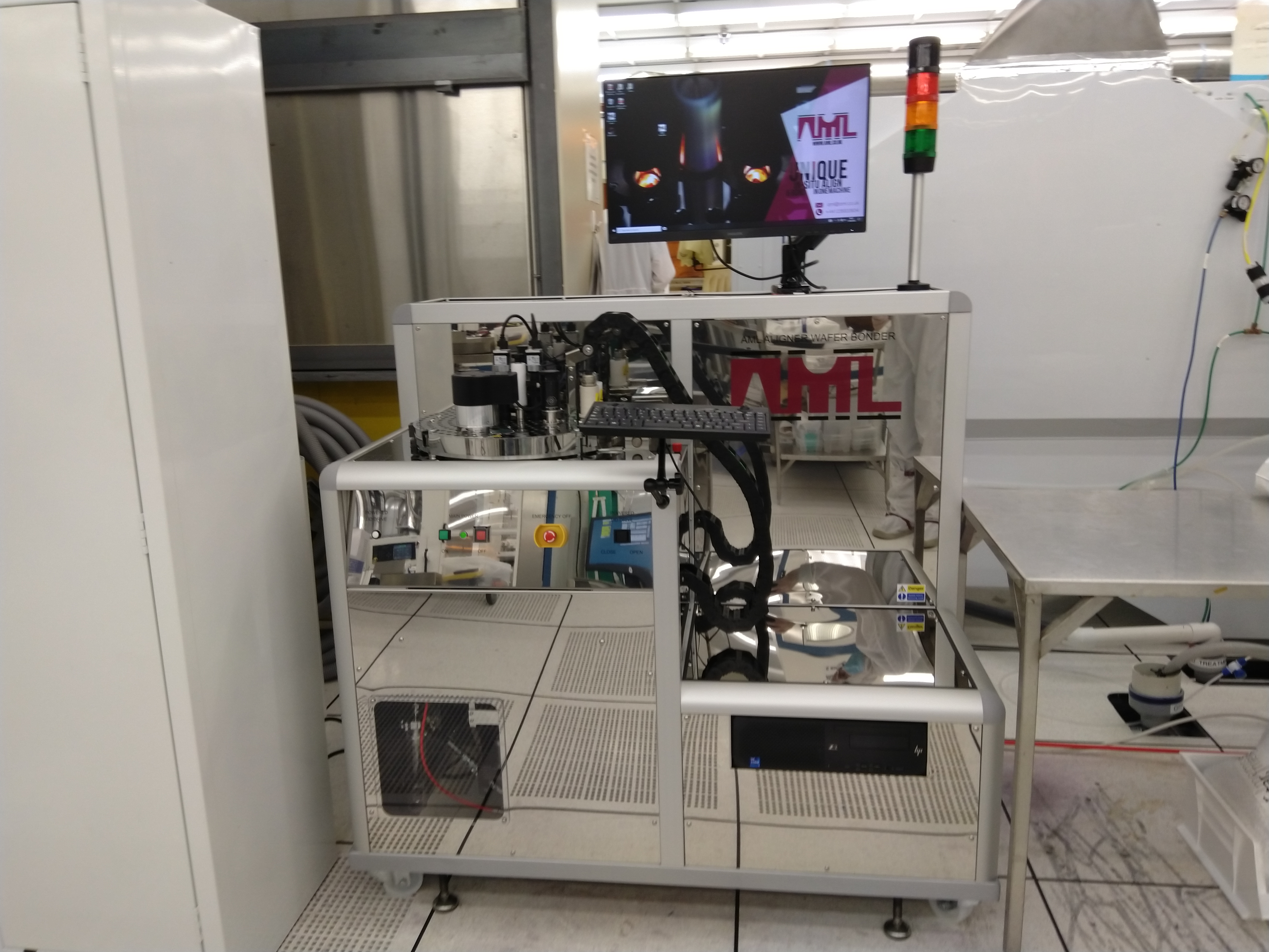
If you are interested in using the AML wafer bonder in your work, please submit a request through LMACS to receive training. If you have any questions, please feel free to contact Scott Munro or Aaron Hryciw.