


We are pleased to announce that the Renishaw inVia Qontor Confocal Raman Microscope is operational and open for training to all nanoFAB users. The inVia Qontor Confocal Raman Microscope is a flexible Raman instrument with unique real-time focus-tracking capabilities for fast and advanced 2D/3D analysis of samples with flat, uneven, curved, or rough surfaces.
The main features include:
- 3 lasers: 532 nm (50 mW), 633 nm (17 mW) and 785 nm (300 mW)
- Objectives: 5X, 20X, 50X (long Working Distance), 100X
- Minimum stage step size of 50nm
- 2D/3D imaging
- Spatial resolution better than 300 nm (532 nm excitation)
- Axial resolution better than 2 μm
- LiveTrack™ focus tracking technology to maintain optimum focus automatically in real time during data collection and white light video viewing
- Macro Sampling Kit allows analysis of non-standard samples, that includes a 90° adapter to allow analysis of samples mounted at 90° to the optic axis and various holders for vials, NMR tubes, cuvettes and capillary tubes.
If you are interested to submit samples for staff analysis or get trained on the tool, please submit a “sample” or “training” request on LMACS. If you have any questions, please contact Peng Li (Peng.Li@ualberta.ca) – the Characterization Group Manager.
Resolution
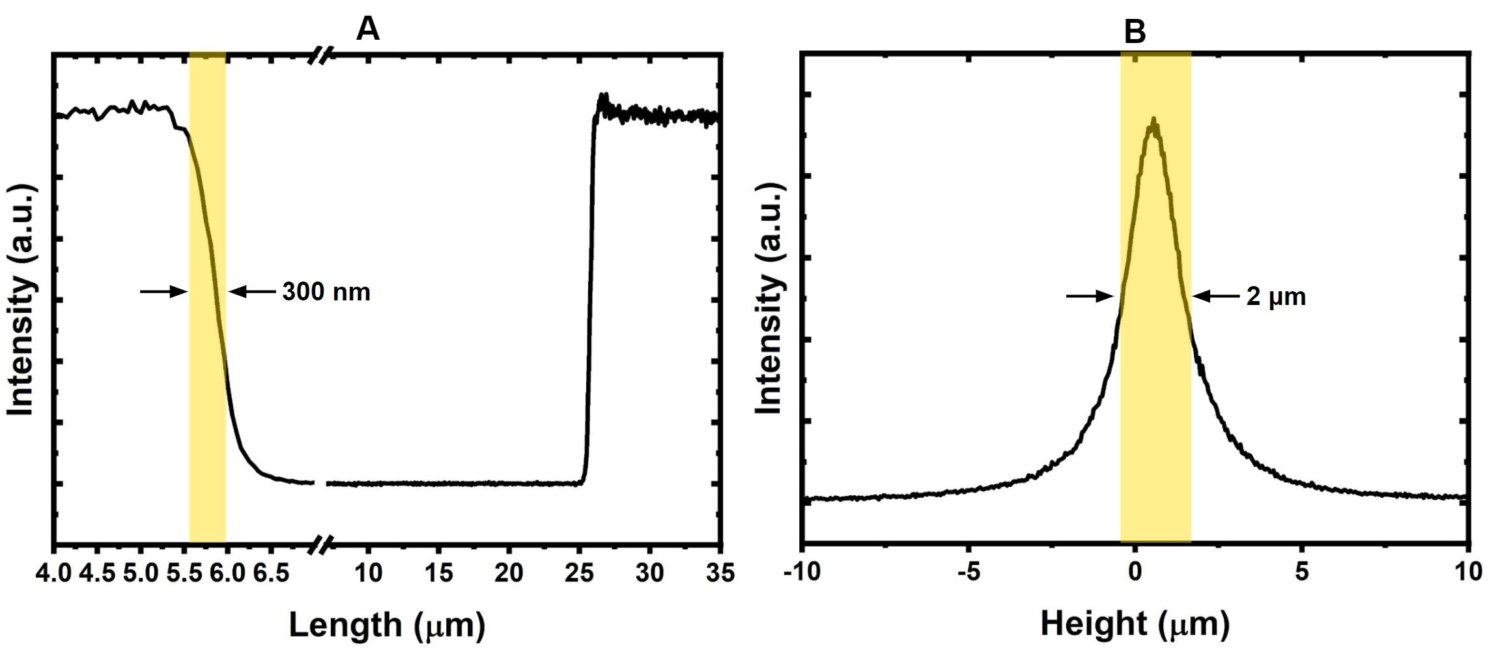
Typical spatial resolution achieved with 532 nm laser and 100X objective: (A) Lateral resolution of 300 nm measured from edge of Si pattern; (B) Confocal / Z-axis resolution of 2 μm measured from FWHM of confocal depth profile from Si surface.
Live Track
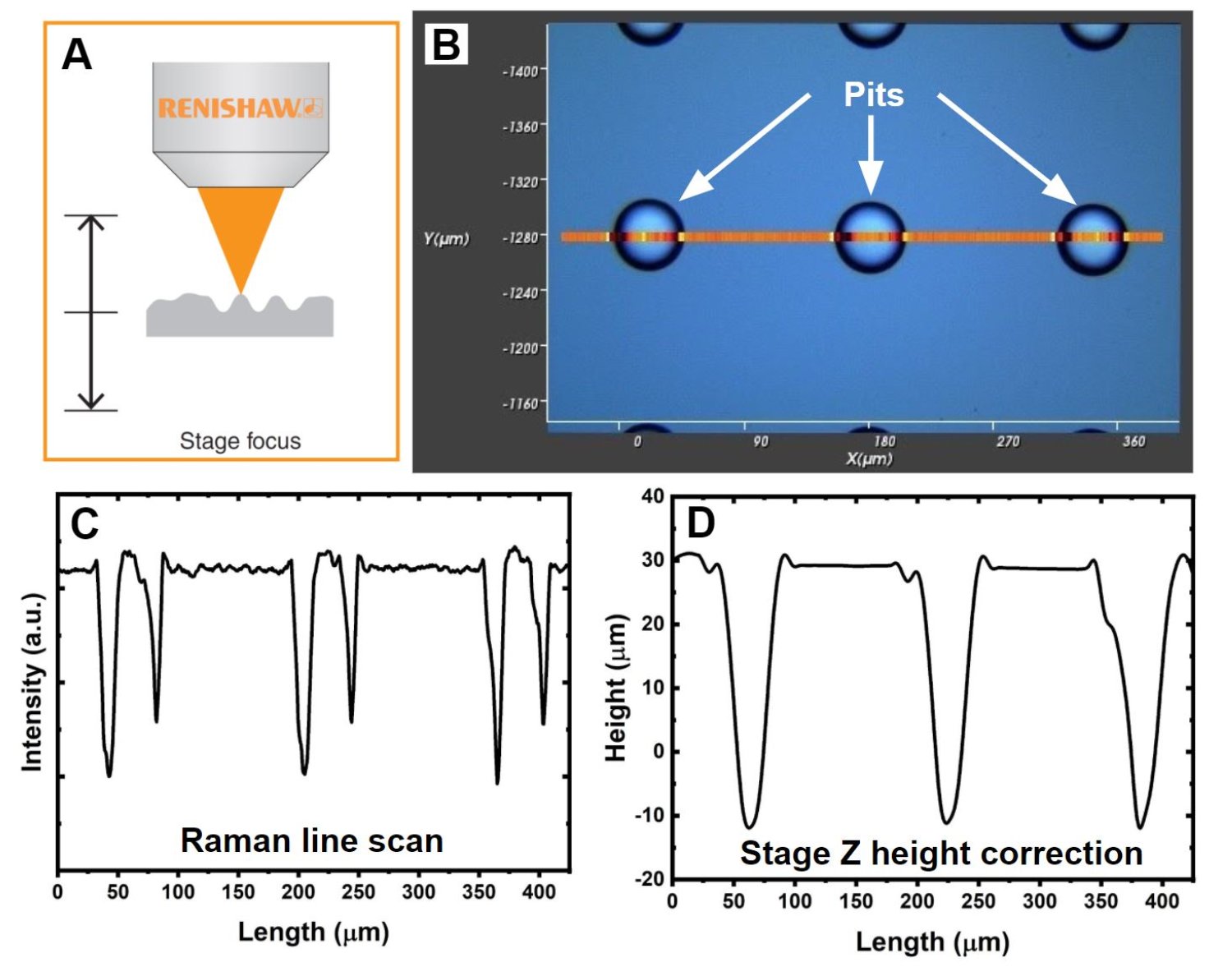
Live track test results from a patterned Si substrates: (A) the motorized stage height is continually adjusted to maintain focus during viewing and scanning; (B) Optical images of Si patterned with 40 μm deep pits; (C) Raman line scan showing same Si peak intensity at the surface and bottom of the pits; (D) Profile of stage Z height correction
2D-Mapping
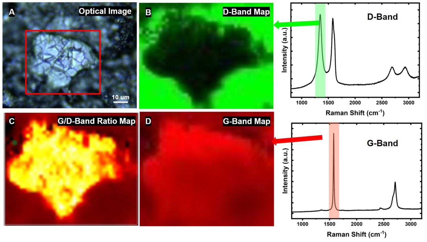
Flexible mapping capabilities showing different phases of Graphene and their distributions: (A) Optical image; (B) D – Band Map; (C) G/D – Band Ratio Map; (D) G – Band Map
Large area mapping of metal (Cr) patterns on Si substrate: (A) stitched optical images; (B) Raman mapping – Yellow/Si and Cyan/Cr.
3D-Mapping

3D mapping and depth profile of a film stack consisting of Laminate film, Parylene and Parafilm
In-Situ Raman

Automatic in-situ Raman acquisition of carbon electrode materials in a K-ion battery cells during discharge and charge cycle. Sample Courtesy: Drs. Keren Jiang and Zhi Li, CME, University of Alberta