The nanoFAB is pleased to announce the winners of the 2020 nanoFAB Image Contest. Images were judged on criteria including image quality, technical merit, and overall aesthetic appeal, and voted on by nanoFAB staff members. Congratulations to the winners, and many thanks to everyone who participated!
1st Place
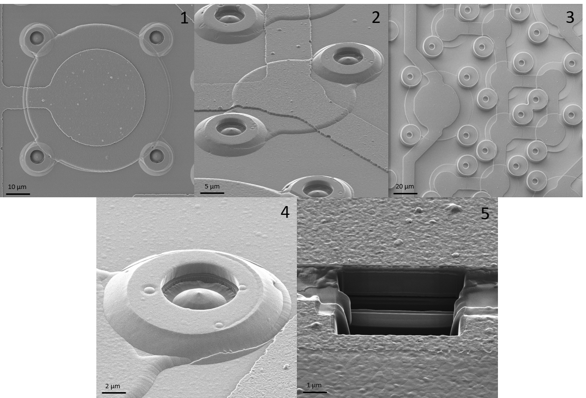
Capacitive Micromachined Ultrasound Transducer (CMUT)
Name: Mohammad Maadi (Roger Zemp Group, Department of Electrical and Computer Engineering, University of Alberta)
Description: These ultrasonic arrays were fabricated completely using the facilities at the nanoFAB. The arrays are then wire-bonded to custom PCB designs and finally become ready for ultrasound imaging unique applications. Multi-frequency CMUT arrays require 6 lithography steps: HMDS, piranha cleans, thermal oxidation, BOE etching, KOH etching, critical point drying, RIE, PECVD, LPCVD, aluminum sputtering, and aluminum etching, along with 80–100 hours of work. These devices were characterized using the Filmetrics system, Alpha-Step IQ profilometer, Keithley semiconductor analyzer, Scanning Electron Microscopy (SEM), Laser Vibrometer, Zygo, Verasonics, Hydrophone measurement and the helium-ion microscope.
Legend:
- The top view of a low-frequency CMUT.
- The top view of a high-frequency CMUT.
- The top view of a interlaced multi-frequency CMUT.
- The sacrificial plugs to release the membranes. The plugs filled by PECVD SiO2 while the top layer is LPCVD SiN.
- Drilled cross-sectional view of a CMUT. The top metal layer is aluminum, which is deposited on a SiN membrane. The membrane is suspended on a 400 nm vacuum gap. The bottom insulator is LPCVD SiN on a highly conductive Si wafer. The device is drilled with Ga gun and imaged with HiM.
2nd Place
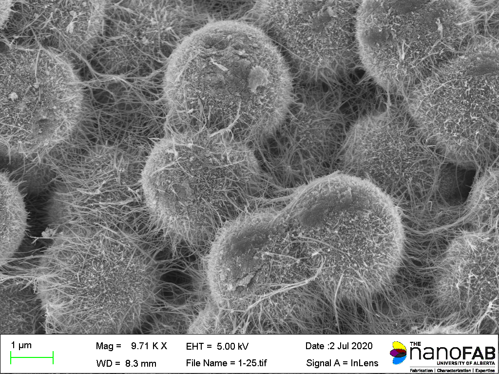
Name: Zhixiao Xu (Xiaolei Wang Group, Department of Chemical and Materials Engineering, University of Alberta)
Description: The material is MnO2 with rambutan-like micro/nano-structure and it is applied as electrode material in aqueous zinc ion batteries for grid-level energy storage. FESEM is used for the imaging this morphology.
3rd Place
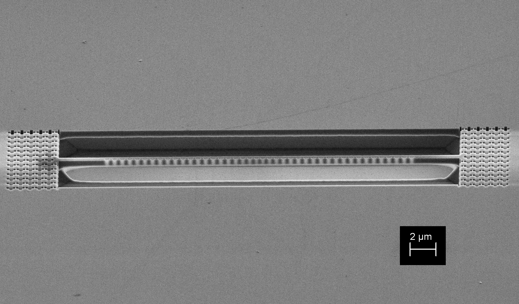
Single-crystal diamond nanobeam fabricated via quasi-isotropic O₂ plasma etching of bulk diamond
Name: Elham Zohari (Paul Barclay Group, Department of Physics and Astronomy, University of Calgary, and John Davis Group, Department of Physics, University of Alberta)
Description: Suspended optomechanical device integrated with one-dimensional photonic crystal cavities and phononic shield from CVD-grown single-crystal diamond enabling photon-phonon interactions as well as coupling of the mechanics to nitrogen-vacancy centre spins. These specimens were fabricated by using quasi-isotropic oxygen plasma etching and imaged with the Zeiss Sigma field-emission SEM. Special thanks to Joe Losby for assisting in the fabrication process.
Runner-up
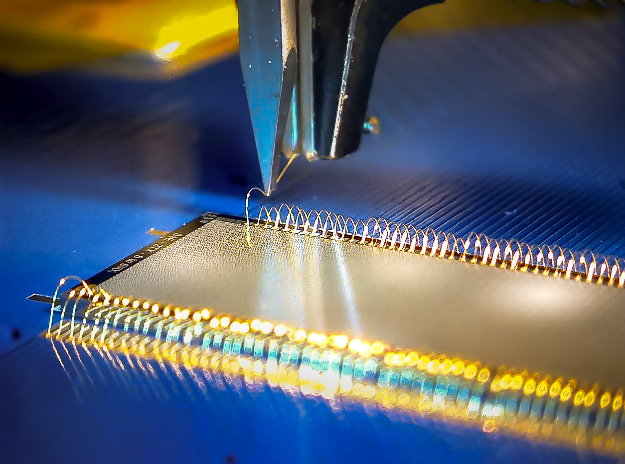
Wire-bonding of Large-Scale CMUT Arrays
Name: Mohammad Maadi (Zemp Group, Department of Electrical and Computer Engineering, University of Alberta)
Description: The image shows the wirebonding of CMUT arrays using the wedge bonder at NINT. These ultrasonic arrays were fabricated completely using the facilities at the nanoFAB. The arrays are then wire-bonded to custom PCB designs and finally become ready for ultrasound imaging unique applications. Multi-Frequency CMUT arrays require 6 lithography steps: HMDS, piranha cleans, thermal oxidation, BOE etching, KOH etching, critical point drying, RIE, PECVD, LPCVD, aluminum sputtering, and aluminum etching, along with 80–100 hours of work. These devices were characterized using the Filmetrics system, Alpha-Step IQ profilometer, Keithley semiconductor analyzer, Scanning Electron Microscopy (SEM), Laser Vibrometer, Zygo, Verasonics, Hydrophone measurement and the helium-ion microscope.

