


The nanoFAB is pleased to announce the winners of the 2018 nanoFAB Image Contest. Images were judged on criteria including image quality, technical merit, and overall aesthetic appeal, and voted on by nanoFAB staff members. Congratulations to the winners, and many thanks to everyone who participated!
1st Place

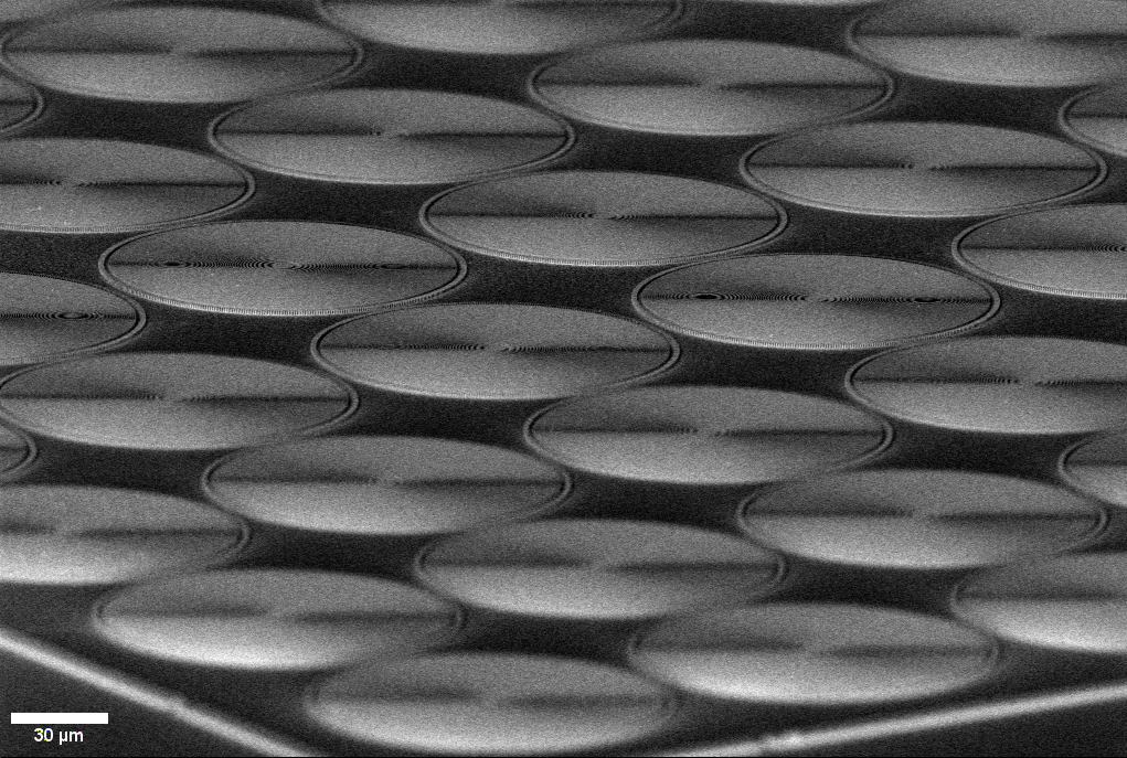
Single-crystal diamond microdisks fabricated via quasi-isotropic O₂ plasma etching of bulk diamond
Name: Matthew Mitchell (Barclay Group, Department of Physics and Astronomy, University of Calgary)
Description: Microdisk optomechanical cavities fabricated from CVD-grown single-crystal diamond that support optical whispering gallery modes, coupled most strongly to the radial breathing mechanical mode of the disk. These specimens were fabricated to investigate cavity optomechanics and diamond colour centre stress coupling.
2nd Place
Phase array of gold patterned Fresnel zone plates
Name: Rob Peters (Applied Nanotools Inc., Edmonton)
Description: This image is an array of gold patterned Fresnel zone plates used for focusing x-rays down to the nanoscale. They use diffraction to focus x-rays, allowing nanoscale imaging x-ray microscopy. The array is used as a phase array. These were fabricated on a thin silicon nitride membrane (100 nm thickness) fabricated in the nanoFAB. The zone plates structures were fabricated using electron-beam lithography and electroplated into the e-beam resist mould, producing the nanoscale rings of the zone plate.
3rd Place
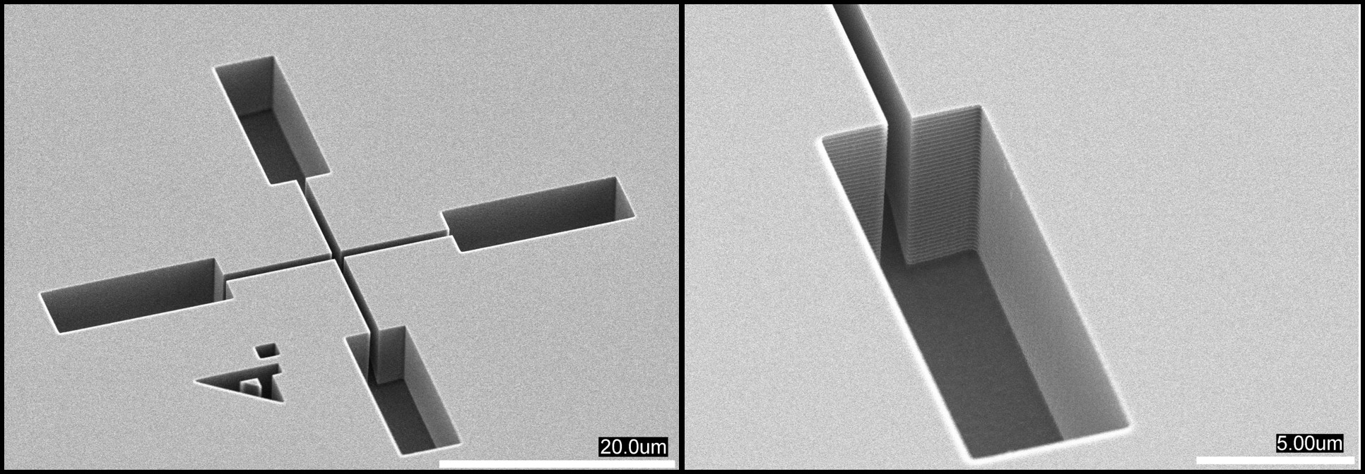
Etched alignment mark
Name: Arash Mohammadpour (Avalon Holographics Inc., St. John’s, NL)
Description: This FESEM image was captured from an alignment mark that was etched into a Si chip. It was used for performing alignment during electron beam lithography (EBL) patterning. nanoFAB’s ICPRIE (Oxford Estrelas DSE) system was used for etching such alignment marks. Fabricated alignment marks allowed us to pattern multilayer devices using EBL with a few nanometer overlay accuracy.