


After a gruelling, rigorous round of judging, the nanoFAB is pleased to announce the winners of the inaugural 2017 nanoFAB Image Contest. All of the images—including the flurry of eleventh-hour submissions—were judged on criteria including image quality, technical merit, and overall aesthetic appeal. Congratulations to the winners, and many thanks to everyone who participated!
1st Place
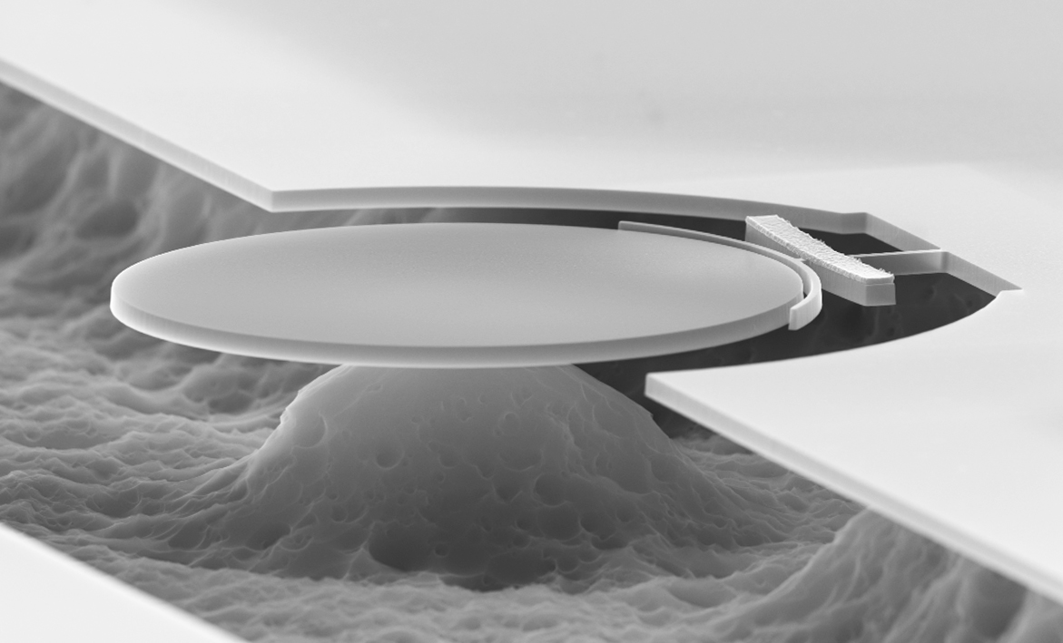
A hybrid optomechancial system, where iron needles are integrated with a sensitive optomechanical torque sensor (0.6 zN·m/√Hz)
Name: Paul Kim (Davis Group, Department of Physics, University of Alberta)
Description: SEM micrograph of an optomechancial system, composed of a 10 µm diameter microdisk coupled to a mechanical oscillator. Two electron-beam lithography steps were used: first e-beam to pattern a small 60 nm gap between the optical and the mechanical resonator, followed by a second e-beam step to lift-off iron-needles. One important step here is the use of HF vapour in order to avoid stiction and preserve the iron-needle since liquid BOE etches most magnetic materials. This device was able to magnetically drive and feedback-cool the mechanical element, which was published in Nature Communications. A field emission scanning electron microscope was used to image these devices with excellent resolution.
2nd Place

Field emission scanning electron microscopy image of monodispersed titania nanosphere shells with 250 nm diameter and 40 nm shell thickness
Name: Yun Zhang (Shankar Group, Department of Electrical and Computer Engineering, University of Alberta)
Description: Monodispersed TiO2 nanosphere shells fabricated using atomic layer deposition. This material can be used for photocatalysis, photonic crystals, and solar cells.
3rd Place (tie)

HAADF and EDX mapping of an Ir-Ni nanopolyhedron
Name: XueHai Tan (Semagina Group, Department of Chemical and Materials Engineering, University of Alberta)
Description: Ir-Ni nanopolyhedron for application of oxygen evolution electrocatalyst.
3rd Place (tie)
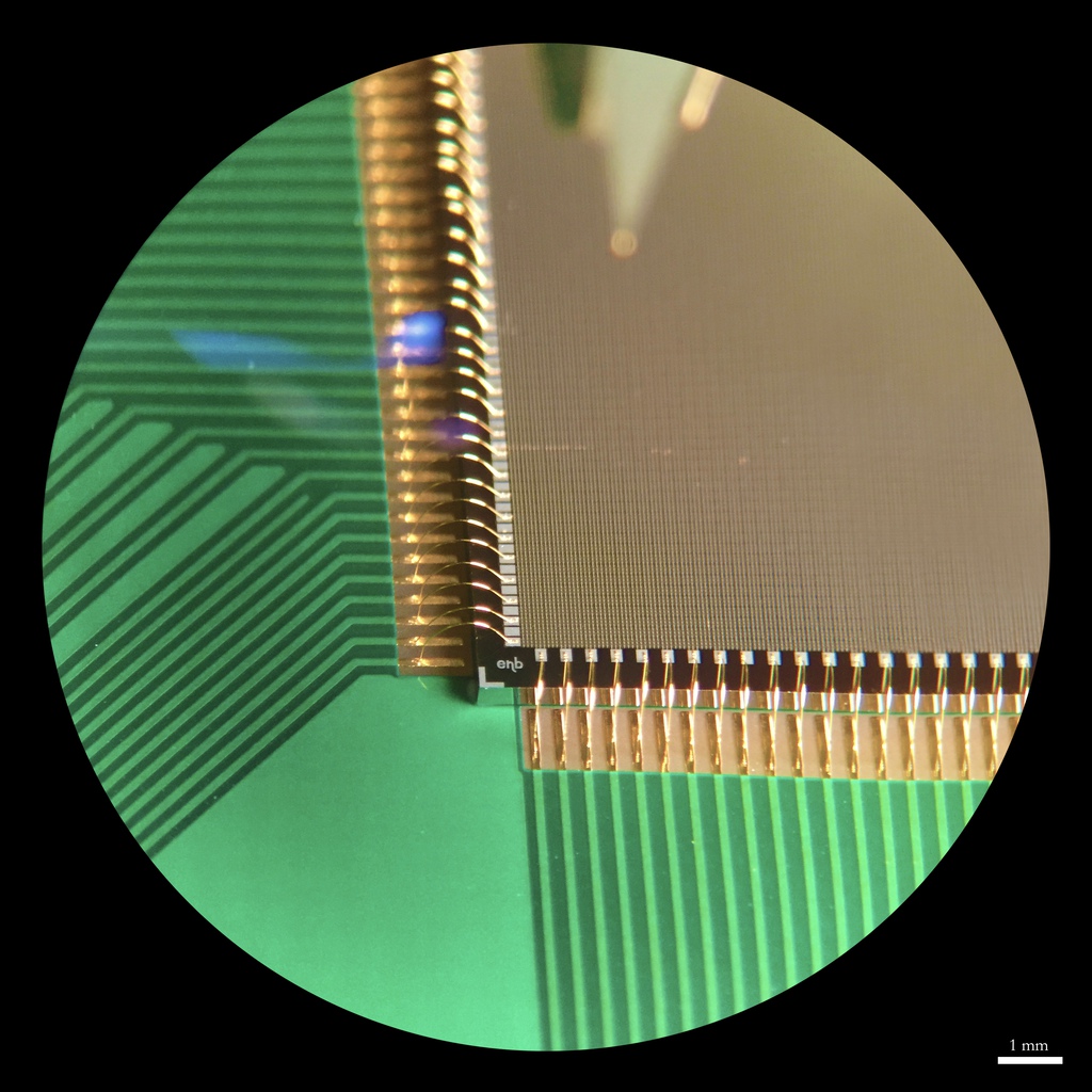
MEMS (some nano assembly required)
Name: Ben Greenlay (Zemp Group, Department of Electrical and Computer Engineering, University of Alberta)
Description: A capacitive micromachined ultrasound array composed of 131,072 isolated silicon nitride membranes, with perpendicular aluminum top electrodes and silicon bottom electrodes. These sensor arrays are capable of high resolution three dimensional imaging, and could represent the future of medical ultrasound imaging. These sensors were fabricated completely using the facilities at the nanoFAB. Each wafer requires 7 lithography steps, HMDS, piranha cleans, thermal oxidation, BOE etching, KOH etching, critical point drying, RIE, PECVD, LPCVD, aluminum sputtering, and aluminum etching, along with 80–100 hours of work. These devices were characterized using the Filmetrics system, Alpha-Step IQ profilometer, Keithley semiconductor analyzer, and the helium-ion microscope.