


The nanoFAB is pleased to invite you to the following workshop, presented by Plasma-Therm, hosted here at the University of Alberta.
- Title: Fundamentals of Plasma Processing (Etching)
- Where: W2-021 ECERF
- Date: Tuesday October 1, 2013
- Time: 8:00 am to 12:00pm

Plasma-Therm Event Flyer
Lectures will include basics of plasma etching mechanisms with relevant examples relating to compound semiconductor, dielectric, metal, and deep silicon etching. State-of-the-art etching technologies for deep silicon will be reviewed. Fundamental and new ideas for endpoint detection and sample thermal budget management will be presented.
The Workshop is intended to provide understanding and insight to those working with plasma etching processes and equipment. The goal is to help researchers make faster progress on projects requiring plasma processing. The course has been very well received at Harvard, UC Berkeley, UCLA, USF, Notre Dame, Cornell, IMRE (Singapore), Lund (Sweden), ISCAS, UCSB, Stanford, SINANO, and UT Austin. Graduate students, post docs, professors, and staff have all found the material useful. Please be assured that the course is not an advertisement about Plasma-Therm products.
Speaker Information - David Lishan, Ph.D.
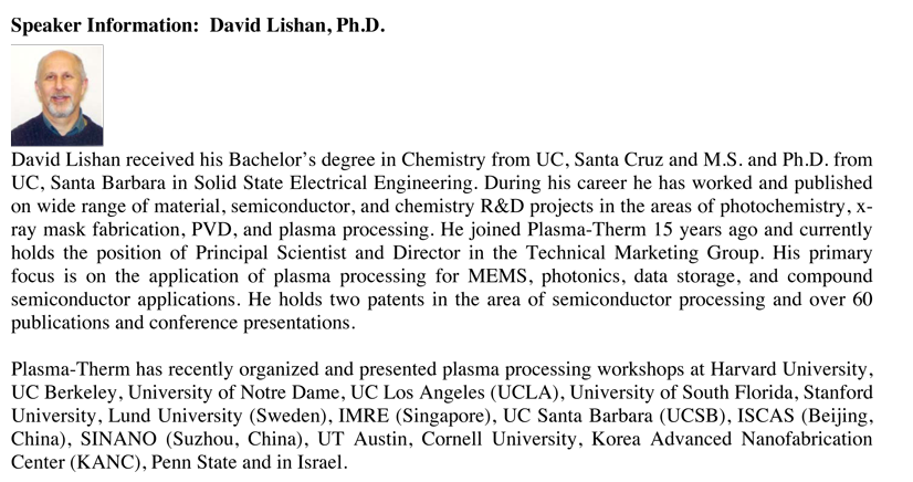
David Lishan, Ph.D
Please note that although this is a free event, online registration is required by September 30 as space is limited. – Register Online
- Continental breakfast will be provided
- Univ of Alberta – Plasma-Therm Workshop flyer and agenda (pdf version)