Articles & News

| |

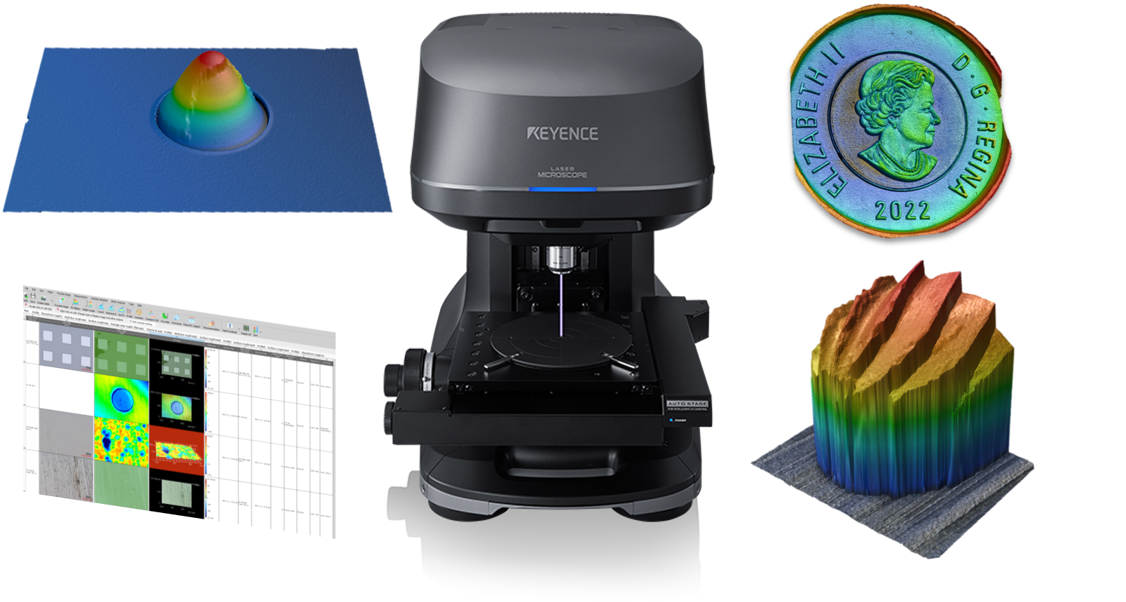
Optical Profilometry Unlimited - Keyence VK-X3050 3D Surface Profiler

Multi-mode Optical Profilometer: Confocal, White Light Interferometry, and Focus Variation.

Josh Perkins
2026-03-09
Read Post
A 3D laser microscope is shown surrounded by examples of 3D surface scans, profilometry images of a coin with colored height mapping, 3D graphs, and analysis software screenshots.
| |

AML Wafer Bonder now available for training

Advanced wafer bonding capabilities are now available using the AML AWB-04

Scott Munro
2024-03-28
Read Post
| |

New Spray Coating Tool Available

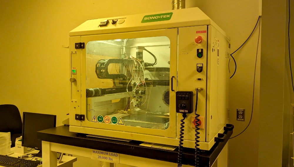
Spray coating of photoresist is now available at the nanoFAB

Breanna Cherkawski
2024-02-02
Read Post
| |

Career opportunity - icspi

Apply for job openings at icspi

Aaron Hryciw
2026-06-16
Read Post
| |

Stealth Dicing: Now at the nanoFAB!

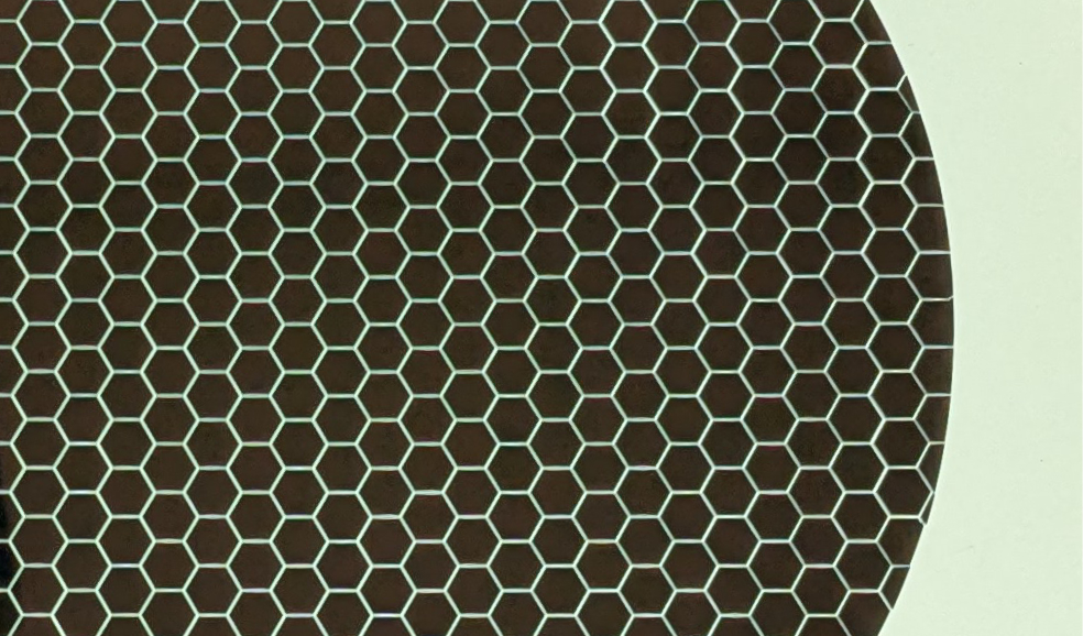
Stealth dicing of Si wafers is now available as a service at the nanoFAB

Breanna Cherkawski
2026-05-07
Read Post
| |

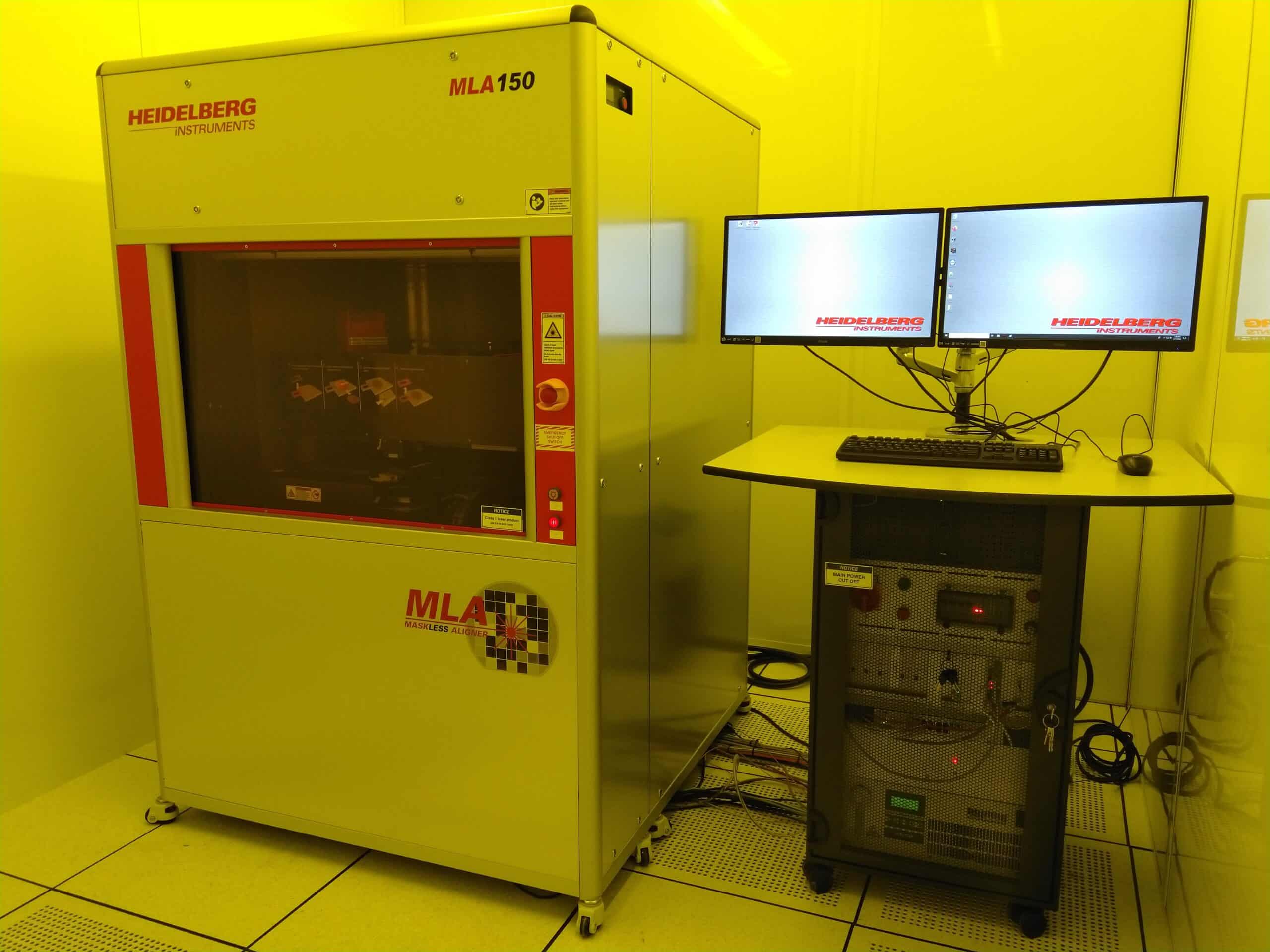
Field alignment now available on the Heidelberg MLA150

Improve your DWL alignment precision with new field alignment capability

Gustavo de Oliveira Luiz
2025-10-23
Read Post
Heidelberg MLA150
| |

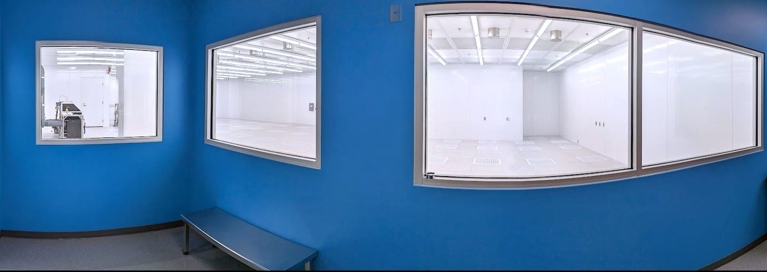
nanoFAB Unveils Cleanroom Expansion

The University of Alberta nanoFAB Centre is proud to announce the successful completion of its cleanroom expansion.

nanoFAB
2025-06-30
Read Post
| |

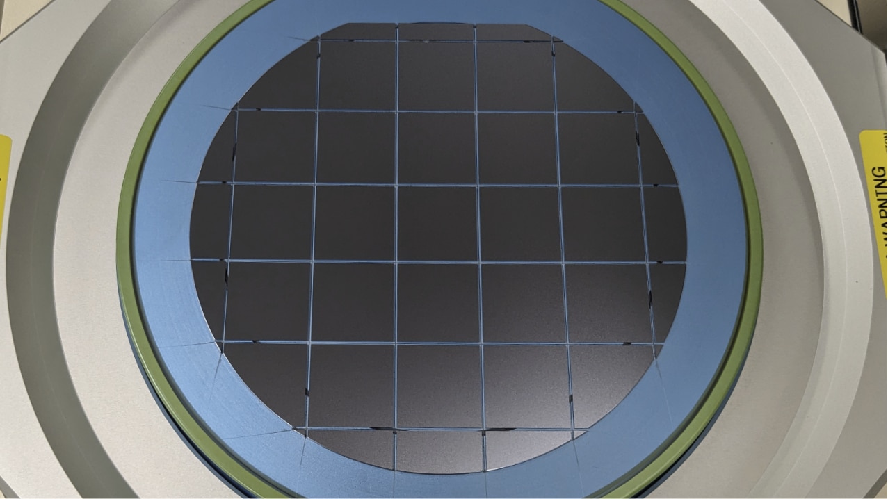
New Die Matrix Expander Available

Improve your dicing post-processing with our new die matrix expander

Breanna Cherkawski
2024-10-30
Read Post
Diced silicon wafer on a die matrix expander tool
| |

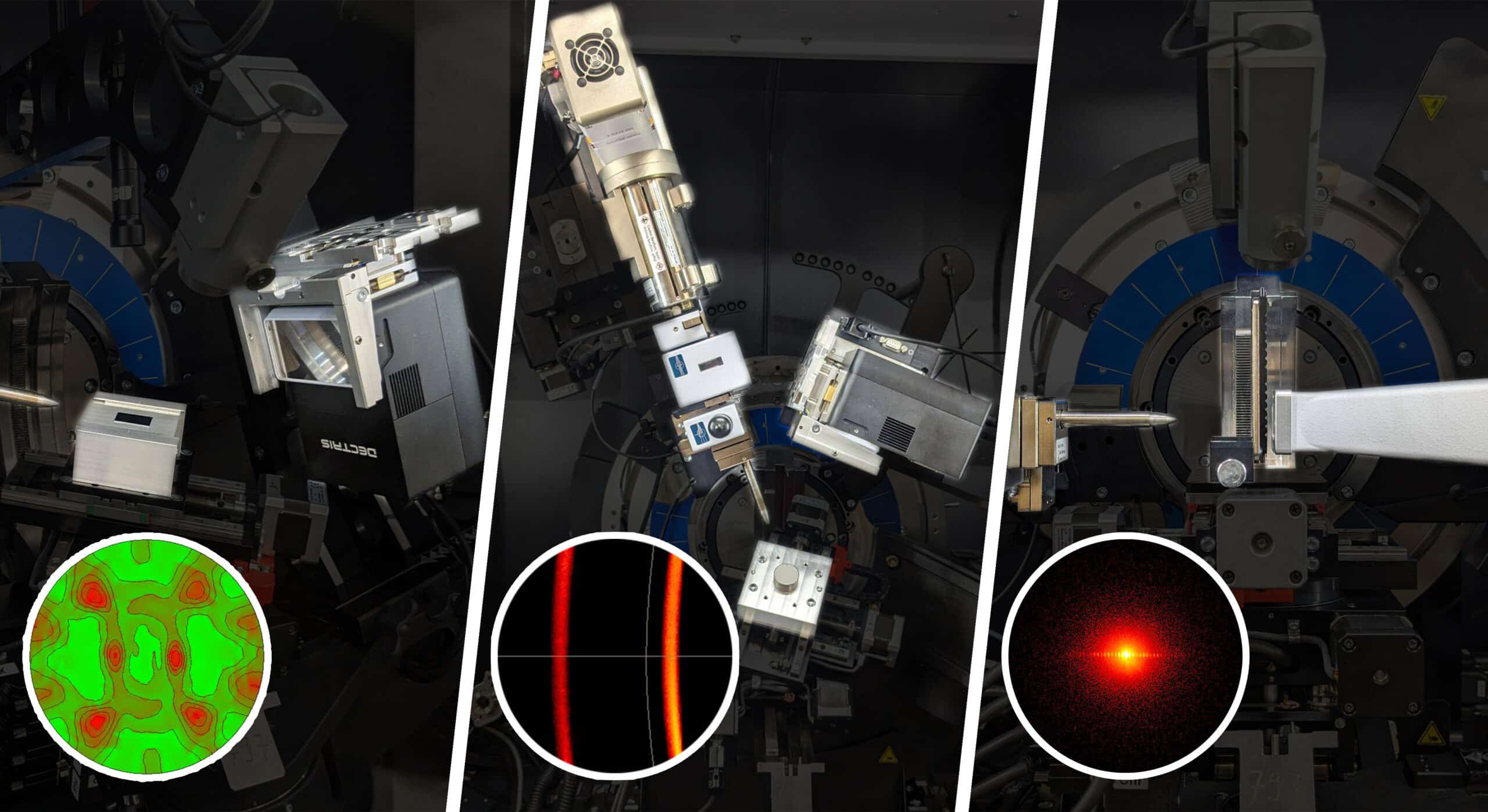
Advanced XRD techniques and applications on Bruker D8D plus diffractometer

Non-Coplanar Scan, Pole Figure, 2D Stress Measurement, and Multi-Angle Scattering

Xuehai Tan
2024-10-01
Read Post
| |

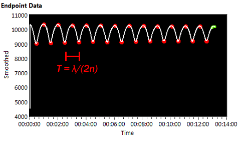
Optical Emission Interferometry (OEI) in the Plasma-Therm Versaline PECVD

Using endpoint detection in PECVD recipes to improve film thickness accuracy

Timothy Harrison
2024-09-03
Read Post
Graph titled "Endpoint Data" shows an oscillating white line with red and green highlights, likely depicting Optical Emission Interferometry data. The X-axis is time and the Y-axis is smoothed data. A red notation reads "T = λ/(2n)" with a horizontal bracket, possibly showcasing Plasma-Therm analysis.
|

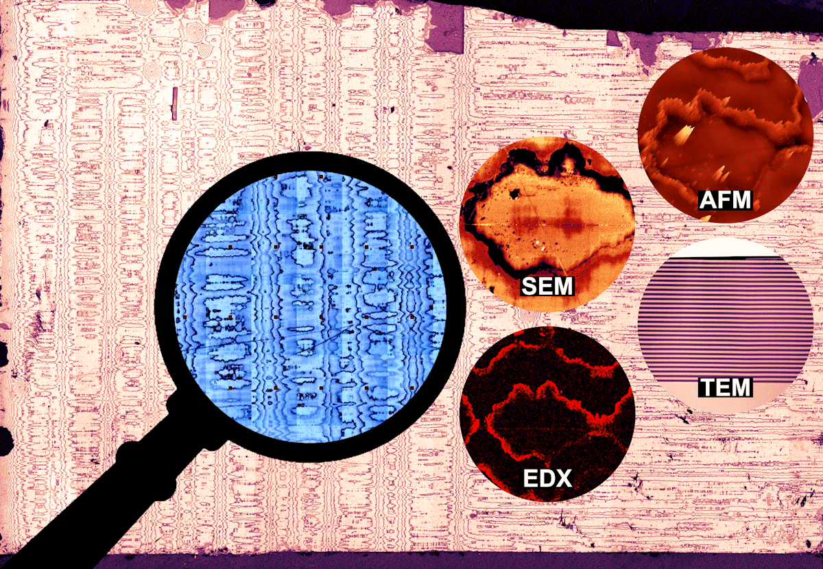
Correlative imaging workflow available on SEM/FIB

The nanoFAB is pleased to announce successful configuration and implementation of software solutions in our electron and ion microscopy, enabling large area imaging and correlative workflow.

Peng Li
2024-06-10
Read Post
A magnifying glass focuses on a textured surface with circular insets labeled AFM, SEM, TEM, and EDX, each showcasing unique patterns and colors. The intricate details highlight the power of correlative imaging to unravel complex structures.
1 2 3 4
hello world!