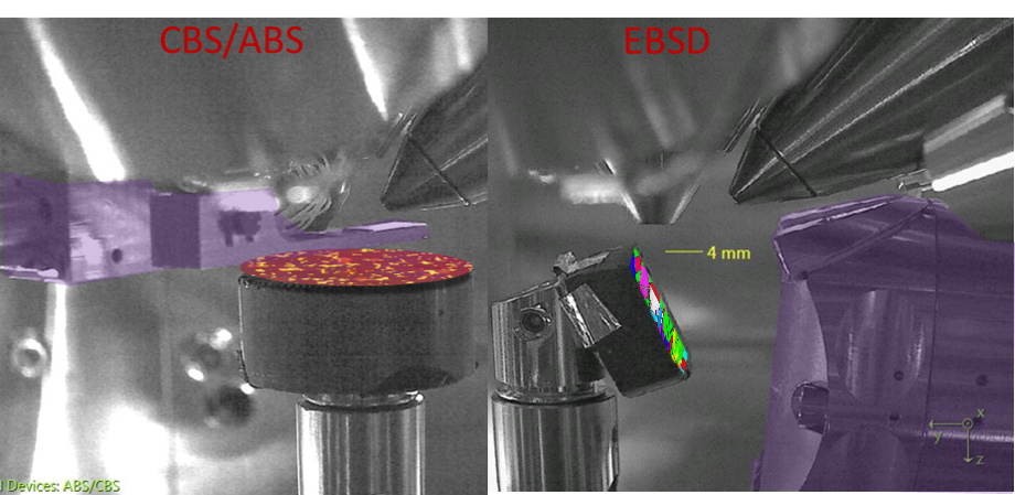
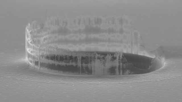
Oxford Symmetry S3 EBSD detector offers high-speed acquisition, enabling large area mapping and co-acquisition with an EDS detector for simultaneous orientation and chemical mapping. Training is now available for the EBSD, EDS, and CBS/ABS modes on the Hydra PFIB/SEM.
The nanoFAB's newly installed KJLC 150LX Atomic Layer Deposition system is now operational and available for training, offering precise, high-quality atomic-scale film growth.
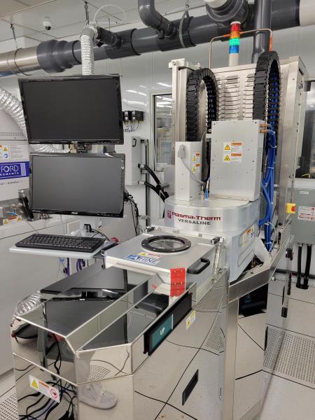
The nanoFAB is pleased to announce that the new Plasma-Therm Versaline PECVD (Plasma-Enhanced Chemical Vapour Deposition) system is fully commissioned and available for user training.
The nanoFAB has successfully commissioned the in-situ testing stage on the Zeiss Xradia Versa 620 X-Ray Microscope, offering advanced mechanical and thermal testing capabilities with enhanced segmentation and deep learning algorithms for superior in-situ analysis.
The nanoFAB is excited to announce the successful installation of the Zeiss ZEISS Xradia Versa 620 X-Ray Microscope, now fully operational for high-resolution, non-destructive 3D microstructure analysis across a variety of fields.
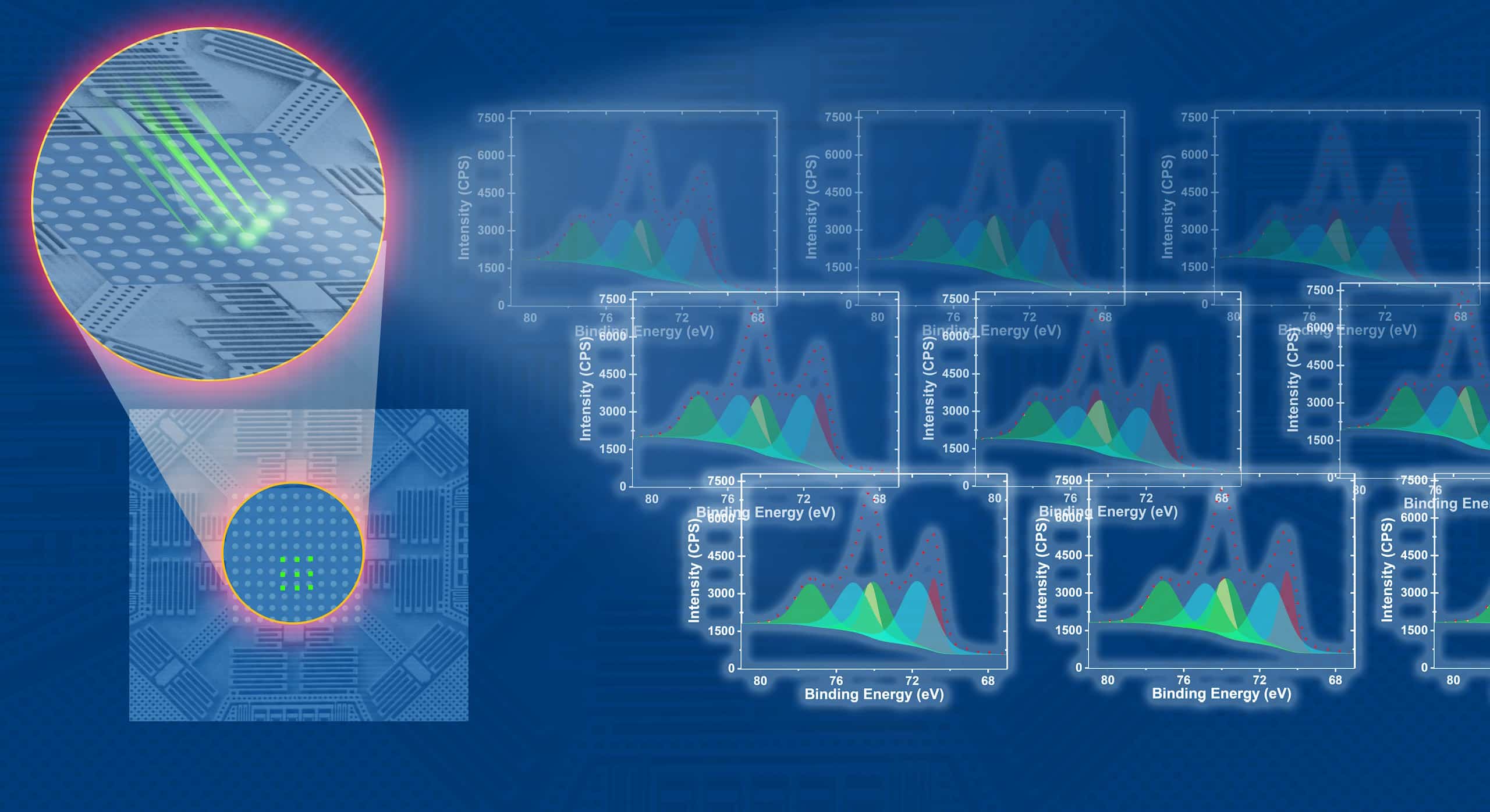
The nanoFAB is pleased to announce that the new PHI VersaProbe III (VP3) Scanning XPS Microprobe has been fully commissioned and all advanced capabilities are open to general access now.
Easily calculate silicon dioxide growth with our new online thermal oxidation calculator, designed to help users determine oxide thickness or oxidation time using industry-standard models for micro/nanofabrication.