



Advanced EBSD + Additional Backscatter modes now available for Training on TF Hydra FESEM
The nanoFAB is pleased to announce the successful installation and deployment of the Oxford Symmetry S3 EBSD detector on the Hydra Helios PFIB/SEM. The S3 detector is a new generation EBSD detector that utilizes CMOS detection instead of CCD, and provides the following advanced capabilities and applications:
- High detection sensitivity
- High acquisition speed (5700 Hz or 5700 patterns per second)
- Unique backscattered images by Forward Scatter Diodes (FSD)
- Large Area Mapping (LAM)
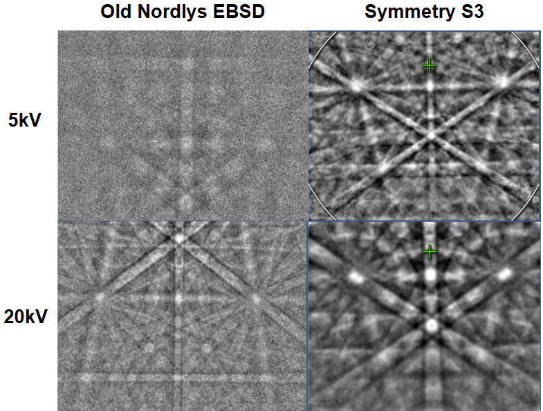
The CMOS detector allows for a significant increase in signal-to-noise ratio (SNR) detection when operating at both low voltages (5 kV) and at typical 15-20 kV voltages needed for Electron Backscattered Diffraction Pattern (EBPS) acquisition. The EBSP acquired by S3 at 5 kV shows sharp, clean, and symmetric bands on single crystal Si, while the old CCD (Nordlys) detector shows poor SNR and low resolution bands operating at low voltages. The improved SNR at low voltages translates to the ability to increase resolution and sensitivity on select samples.
Beyond the SNR enhancement of the S3 and the flexibility in work voltages, the CMOS detection elements enable higher throughput than older CCD-style detectors. Compared to the Nordlys (CCD based) detector, the S3 has an acquisition speed that is 2–3 orders of magnitude higher, with a maximum acquisition speed of 5700 Hz. The increased acquisition speed enables high-throughput sample screening and subsequent higher-resolution scans within a single reservation.
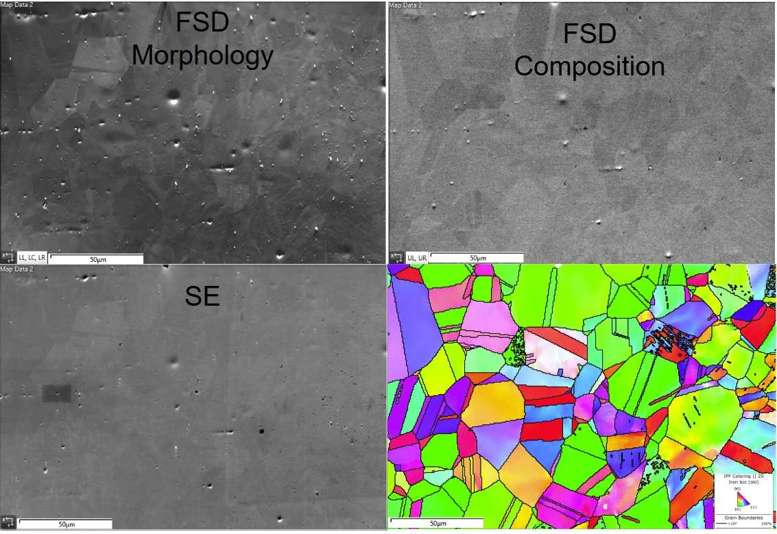
The new generation of detectors is also equipped with Forward Scatter Diodes (FSD) that provides excellent BSD images at high sample tilt angle where normal BSD detectors are highly compromised, which allows for quick estimation of grain size, location, and band contrast without performing a full EBSD scan. The FSD can be utilized in stand-alone or mixed mode to provide contrast to individual grains in an SE-like image.
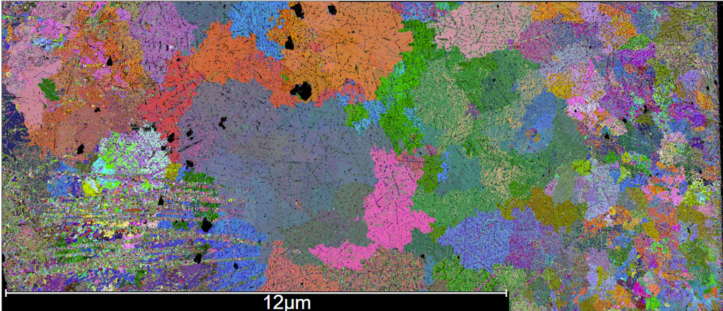
Hydra is not only equipped with an advanced EBSD, but also with advanced software packages. The LAM software package allows users to scan large regions of predetermined zones to quickly survey samples and gather large amounts of data from one sample. This type of acquisition is not feasible with the Nordlys' 13Hz acquisition speed. The S3 detector's speed enables single-site acquisition to be 'arrayed' to analyze much larger zones with high spatial resolution (small stepsize), enabling visualization of large machined parts, printed metals, and long-welds. LAM can also be used in EBSD mode, EDS mode, or even in a coupled EBSD + EDS mode. There is no need to break the vacuum or even position alignment to gain chemical and structural insights about a sample! In the figures below, simple EBSD LAM data can show grain distribution trends or when combined with EDS can give insights into sample preparation performance and chemical/phase segregation. We are pleased to announce that the S3 EBSD, Ultim Max EDX, and LAM functionalities are all available for training on Hydra!
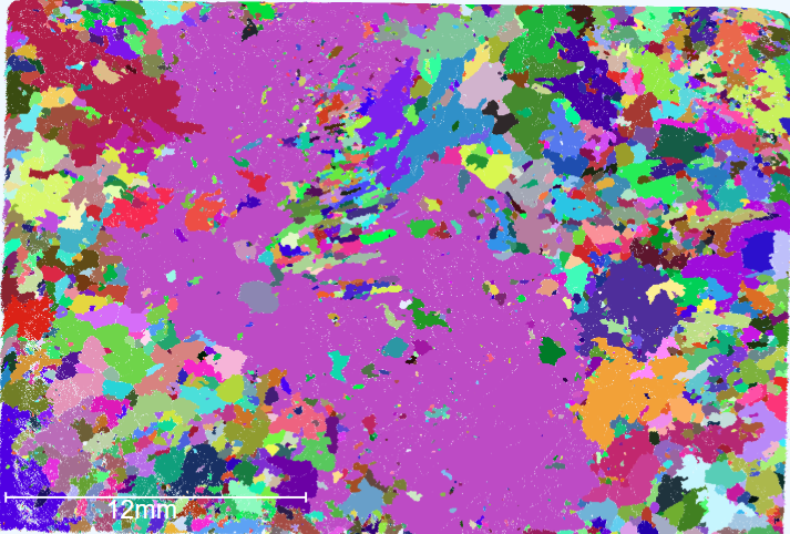
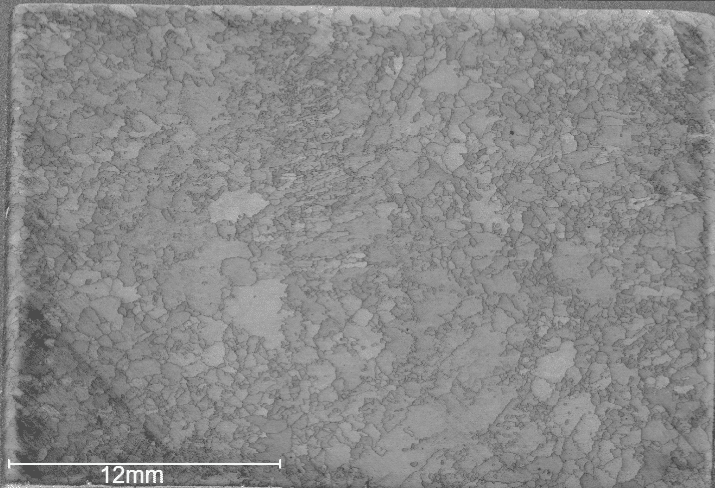
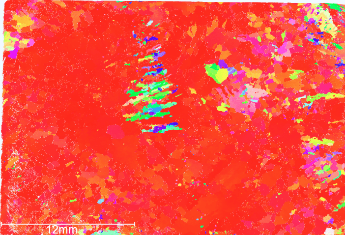
[1] Bulk Inconel, Haoyang Li, ANGAM lab: 800 nm stepsize, 30 minutes total acquisition time.
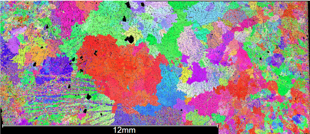
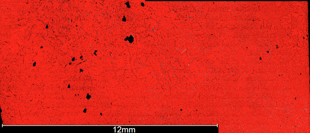
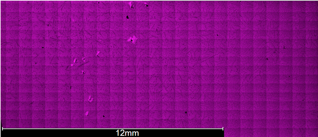
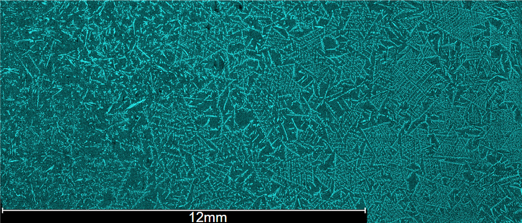
[2] EBSD + EDS maps of CuSn solder, 800 nm stepsize, 4.5 hours total acquisition time.
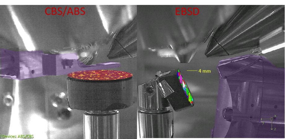
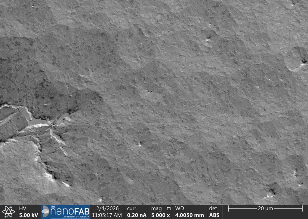
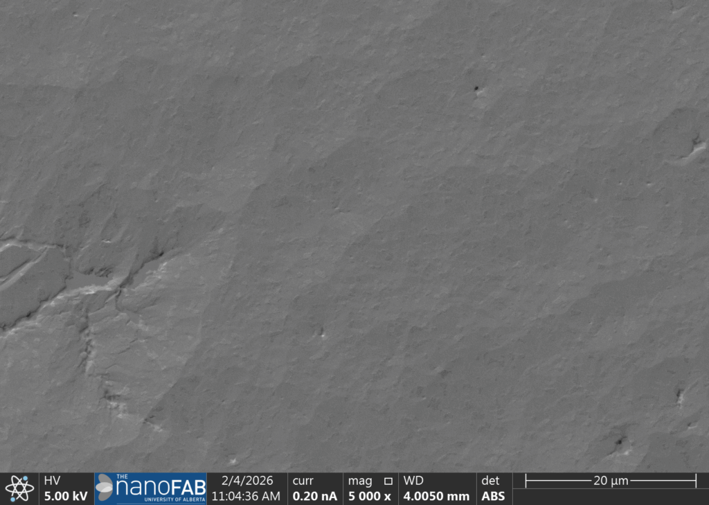
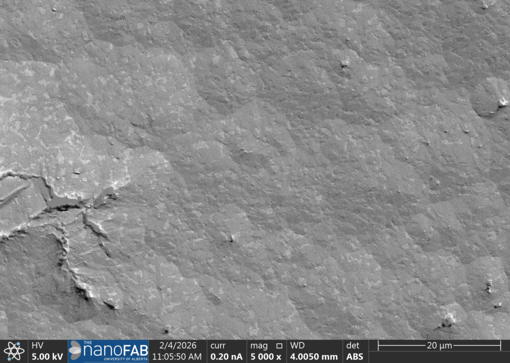
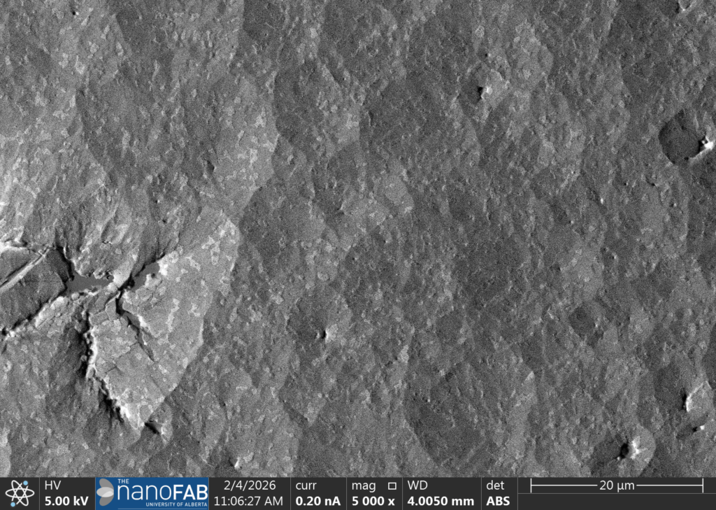
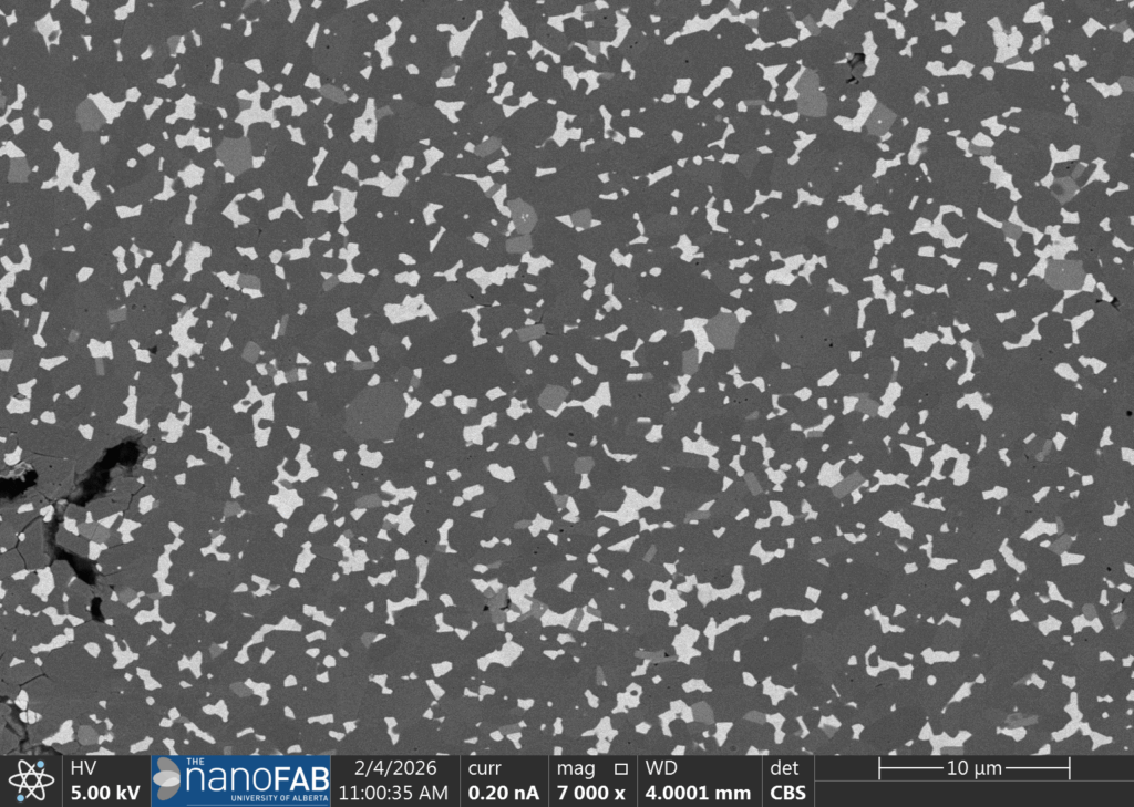
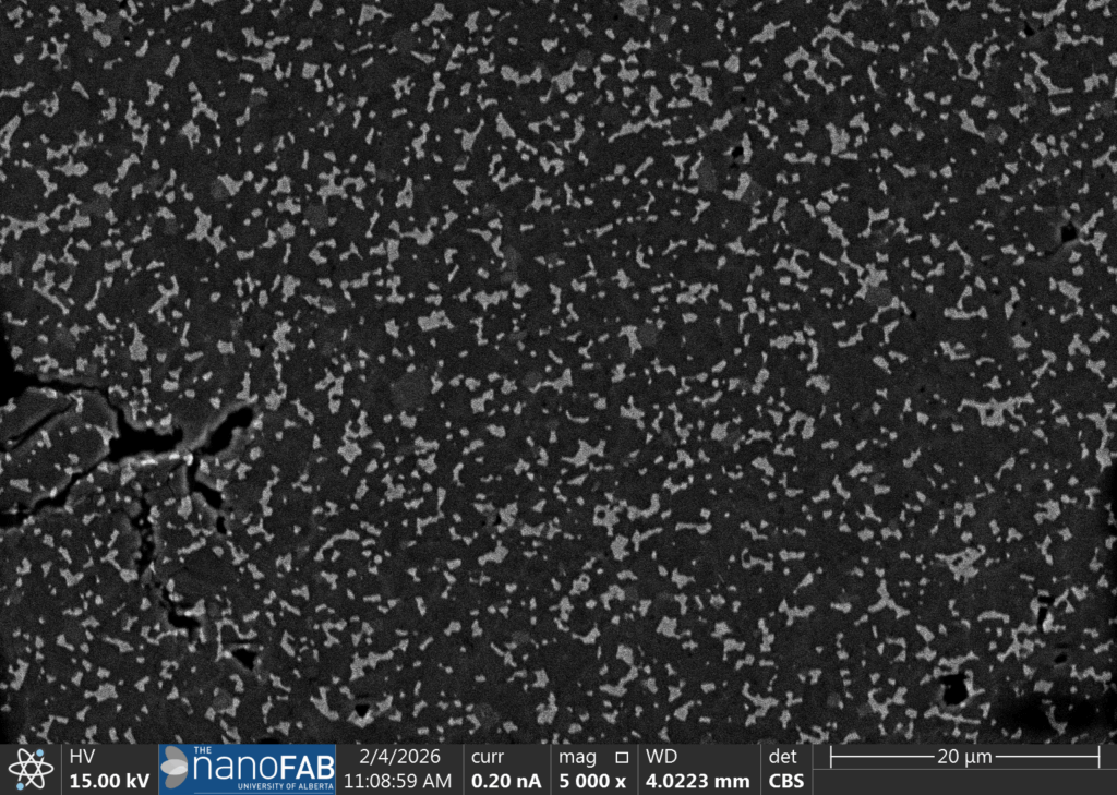
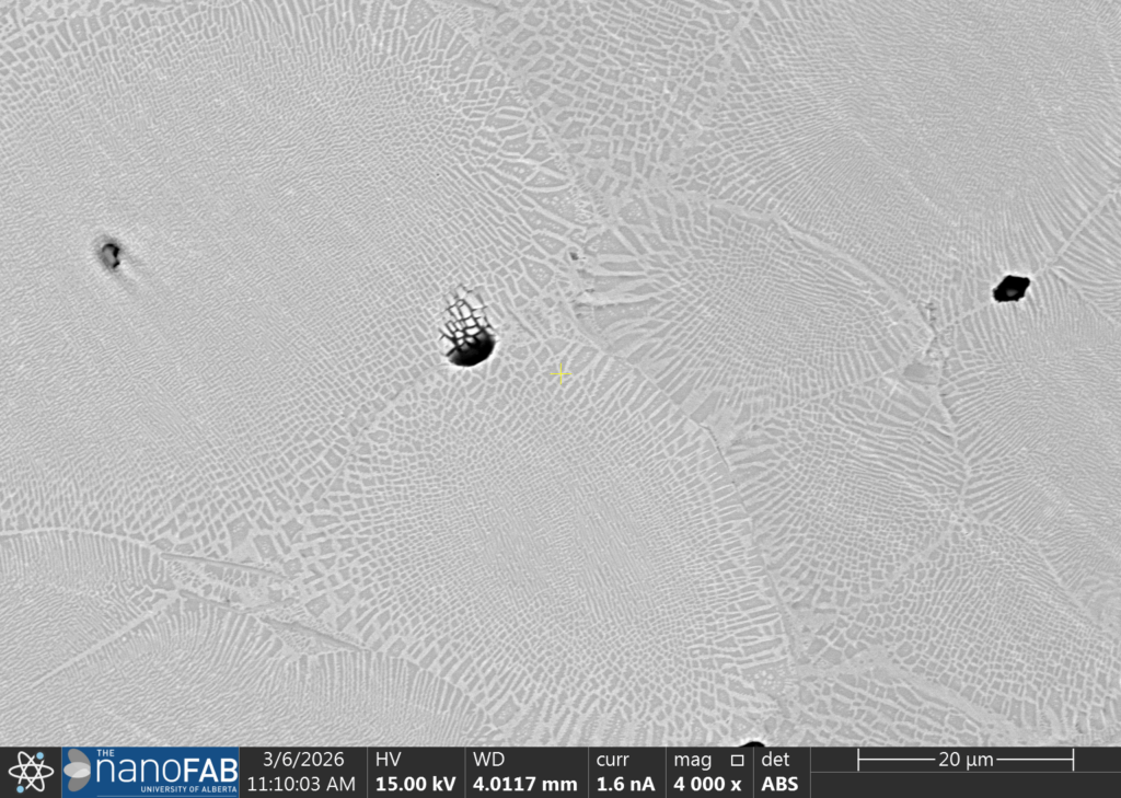
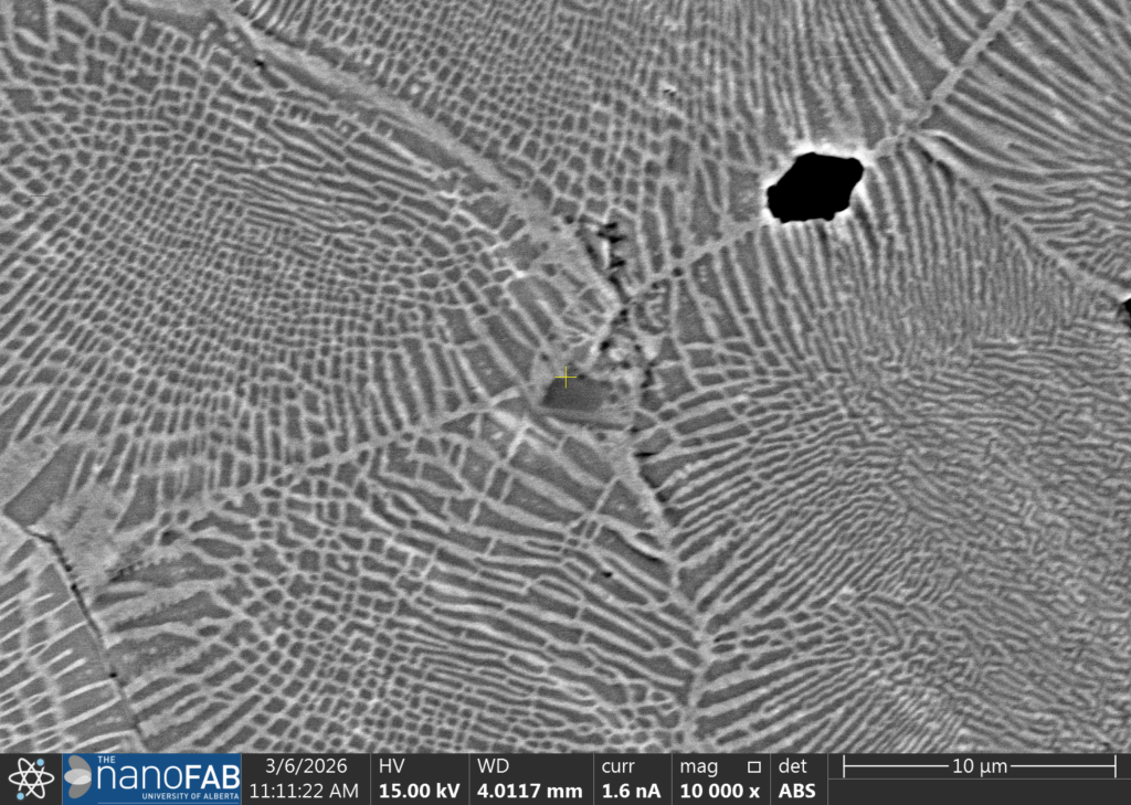
We are also pleased to offer training on the highly sensitive retractable backscatter mode on Hydra as well! Hydras annular backscatter/central backscatter (ABS/CBS) detector is highly sensitive even at low beam current/voltages. The ABS/CBS modes offer material contrast and topographic imaging with configurable detector settings.
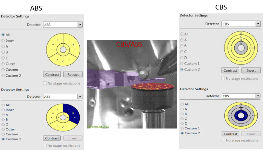
ABS/CBS is a single retractable detector (DBS) that can be utilized in field-free and high resolution immersion SEM modes with variable voltages/currents, allowing for dynamic contrast and inspection. The ABS/CBS inserts between the SEM column and the sample at nominal 4mm working distances. The close proximity of the DBS to the sample allows for high angular extraction of BSE signals at a range of working voltages and currents.
The annular backscatter can be configured to have multiple angularly resolved segments included or subtracted from the signal. ABS mode can be used to highlight 3D topography in a sample. Meanwhile, the CBS can have multiple concentric detector segments included or excluded as part of the analysis to highlight scattering from low-z elements (most outer regions) and high-z atomic contrast in the more central regions. The image gallery below demonstrates the efficacy of the DBS on composite ceramics and metallic materials [3].
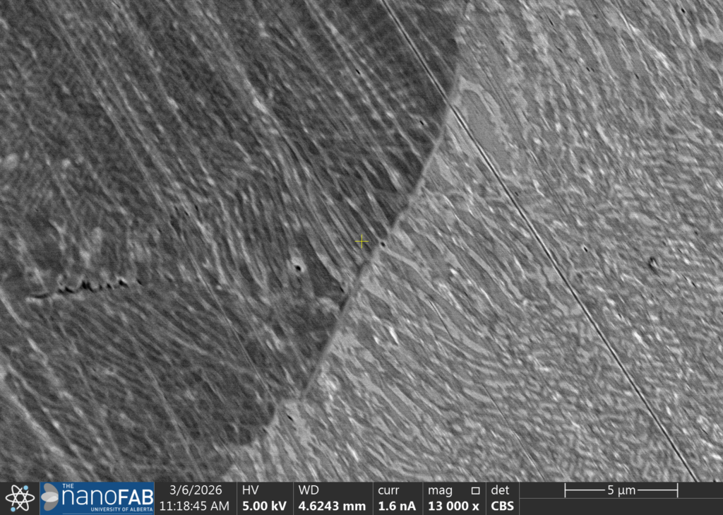
[3] Metallic sample provided by Zhaoqi Chen from Zeng group.