
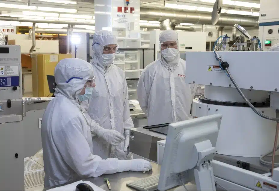
Who can use the nanoFAB? Everyone.
We are an open access nanofabrication & characterization centre.
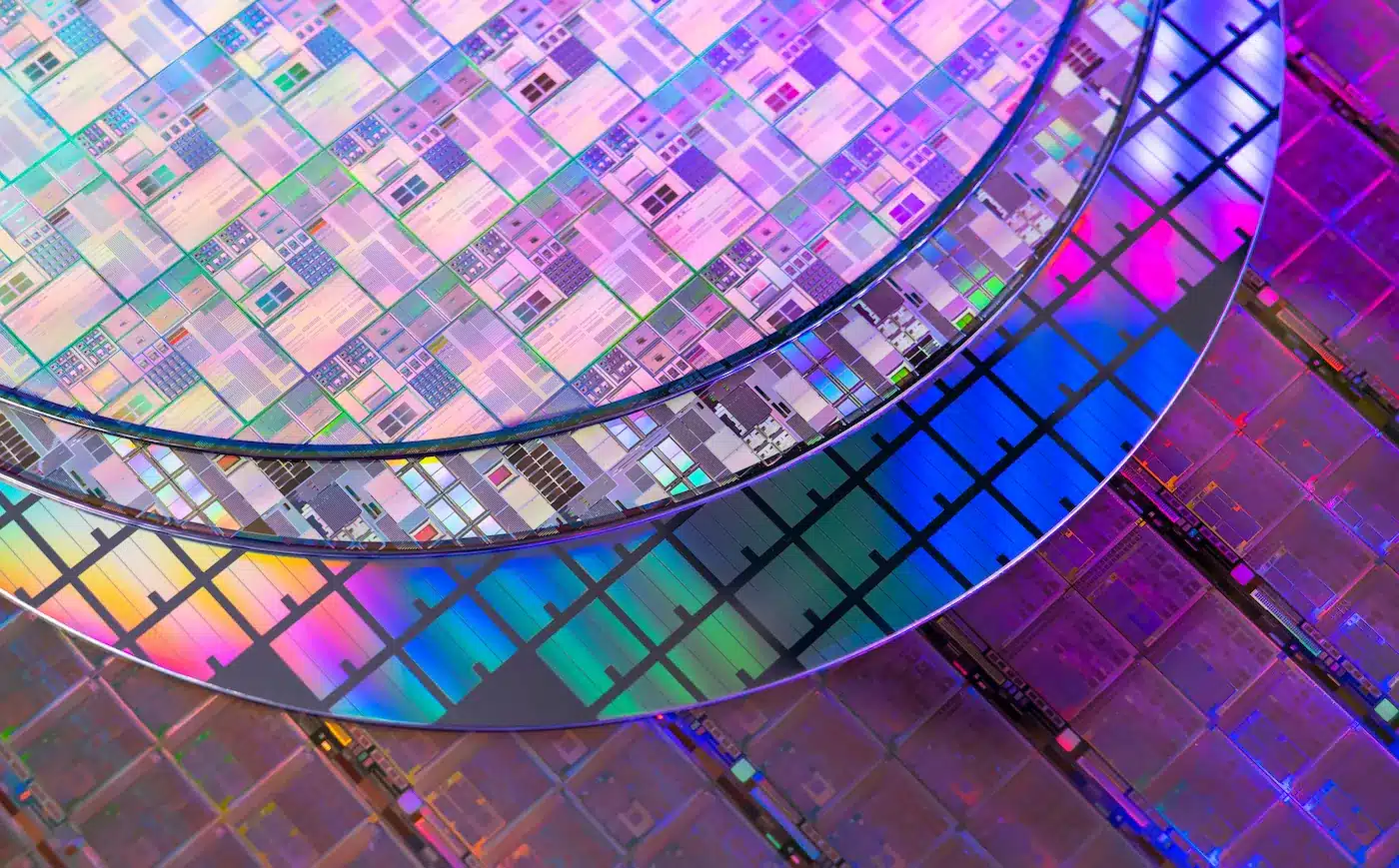
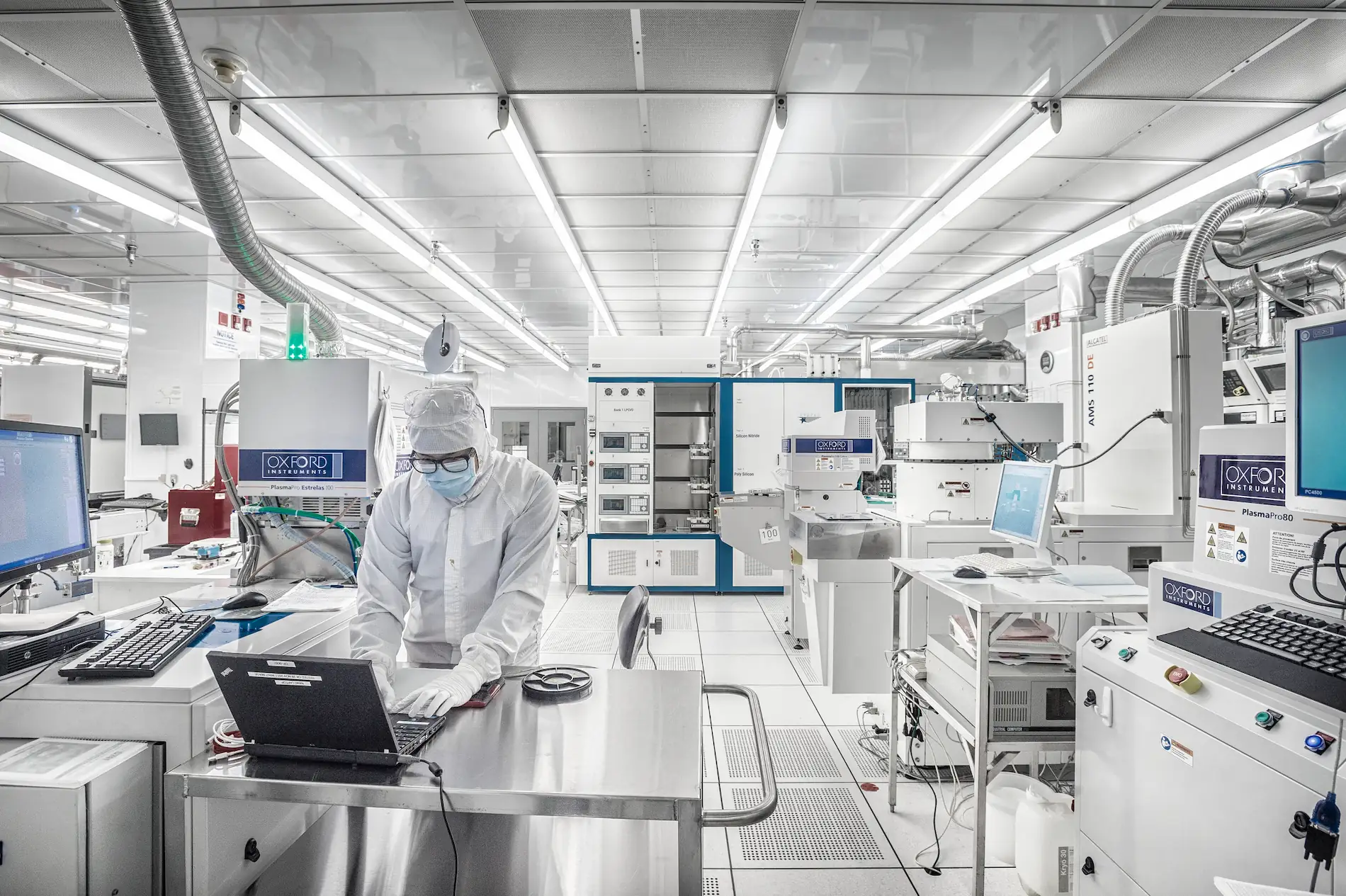
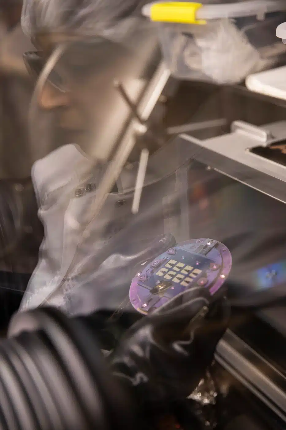
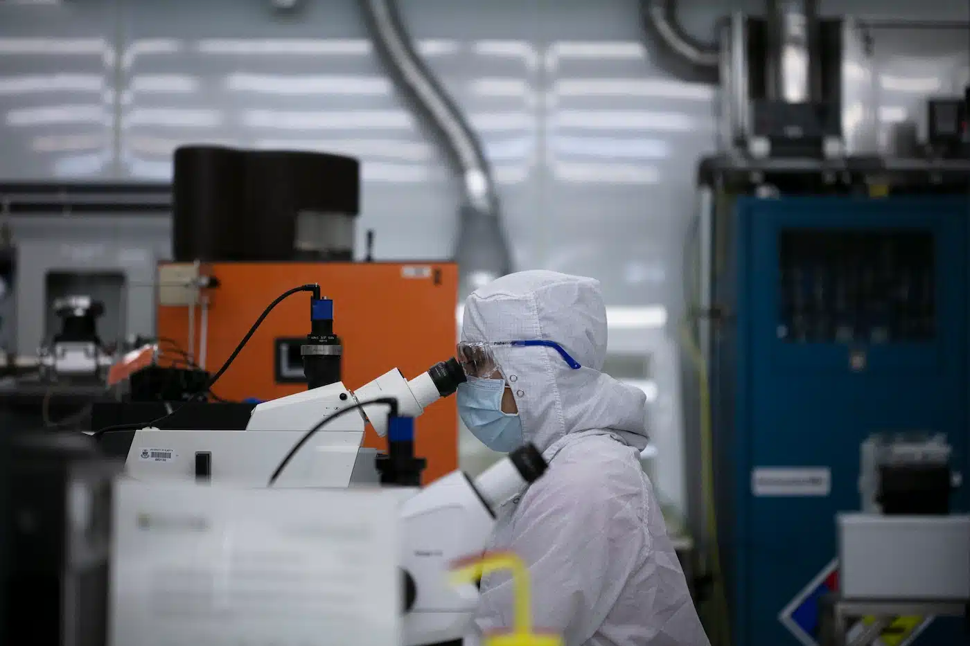
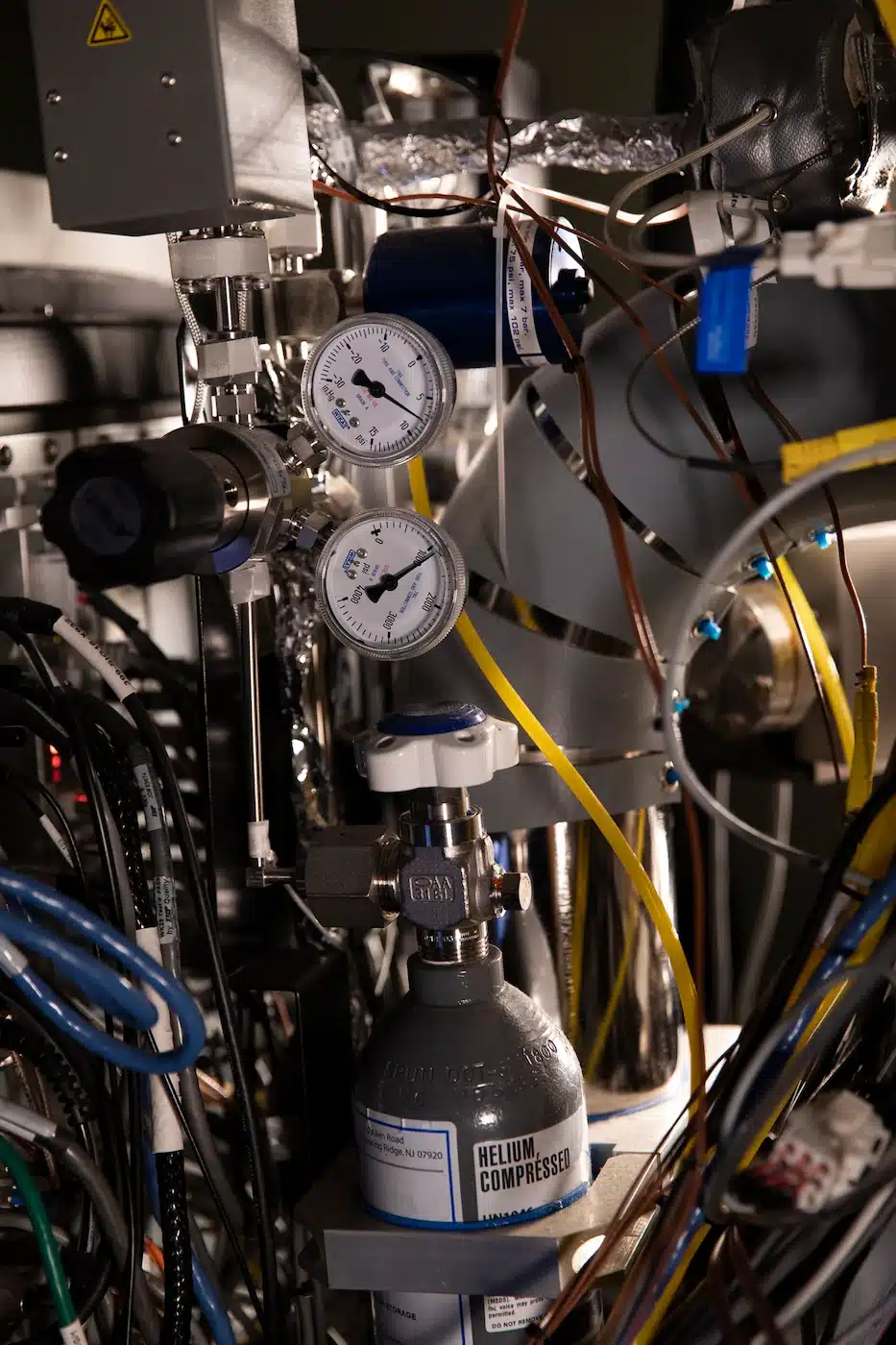
The nanoFAB is a national, open-access training, service, and collaboration centre, focused on academic and industrial applications in micro- and nanoscale fabrication and characterization.


Fabrication | Featured | News
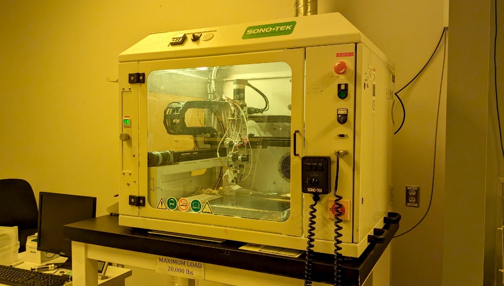
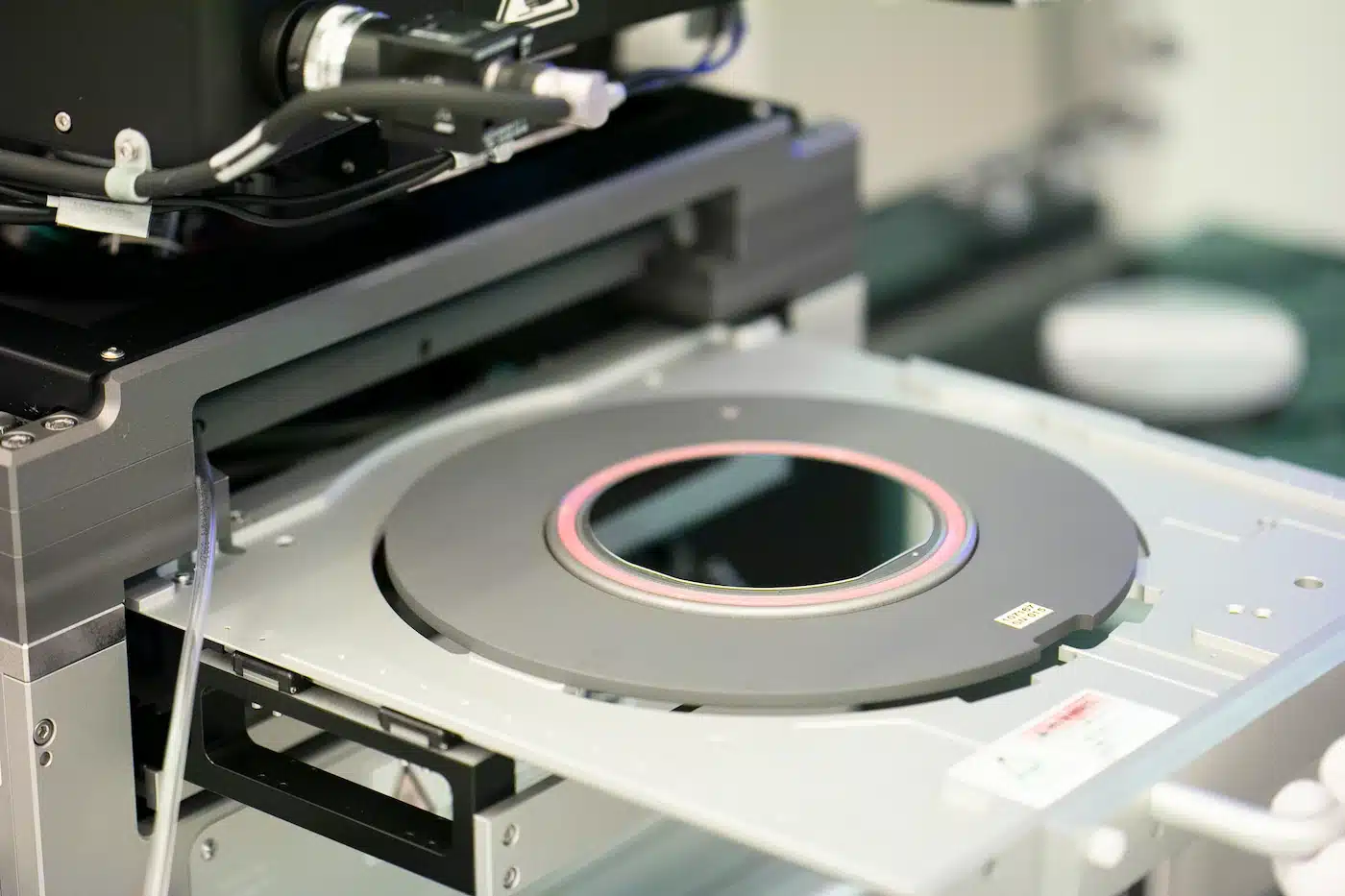
Stealth Dicing: Now at the nanoFAB!
2026-05-07
Stealth dicing of Si wafers is now available as a service at the nanoFAB
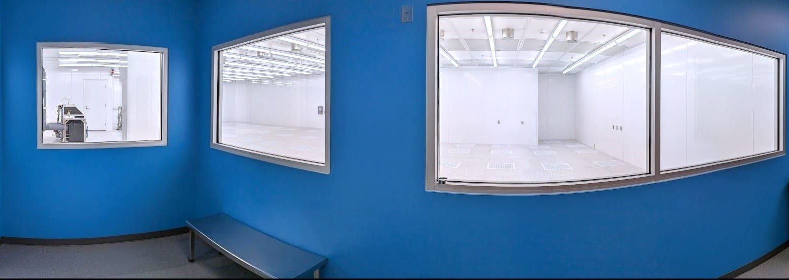
Fabrication | Featured | News
nanoFAB Unveils Cleanroom Expansion
2025-06-30
The University of Alberta nanoFAB Centre is proud to announce the successful completion of its cleanroom expansion.
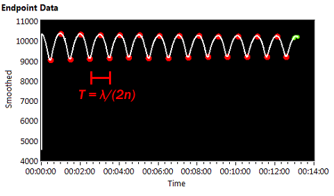
Fabrication | Featured | News
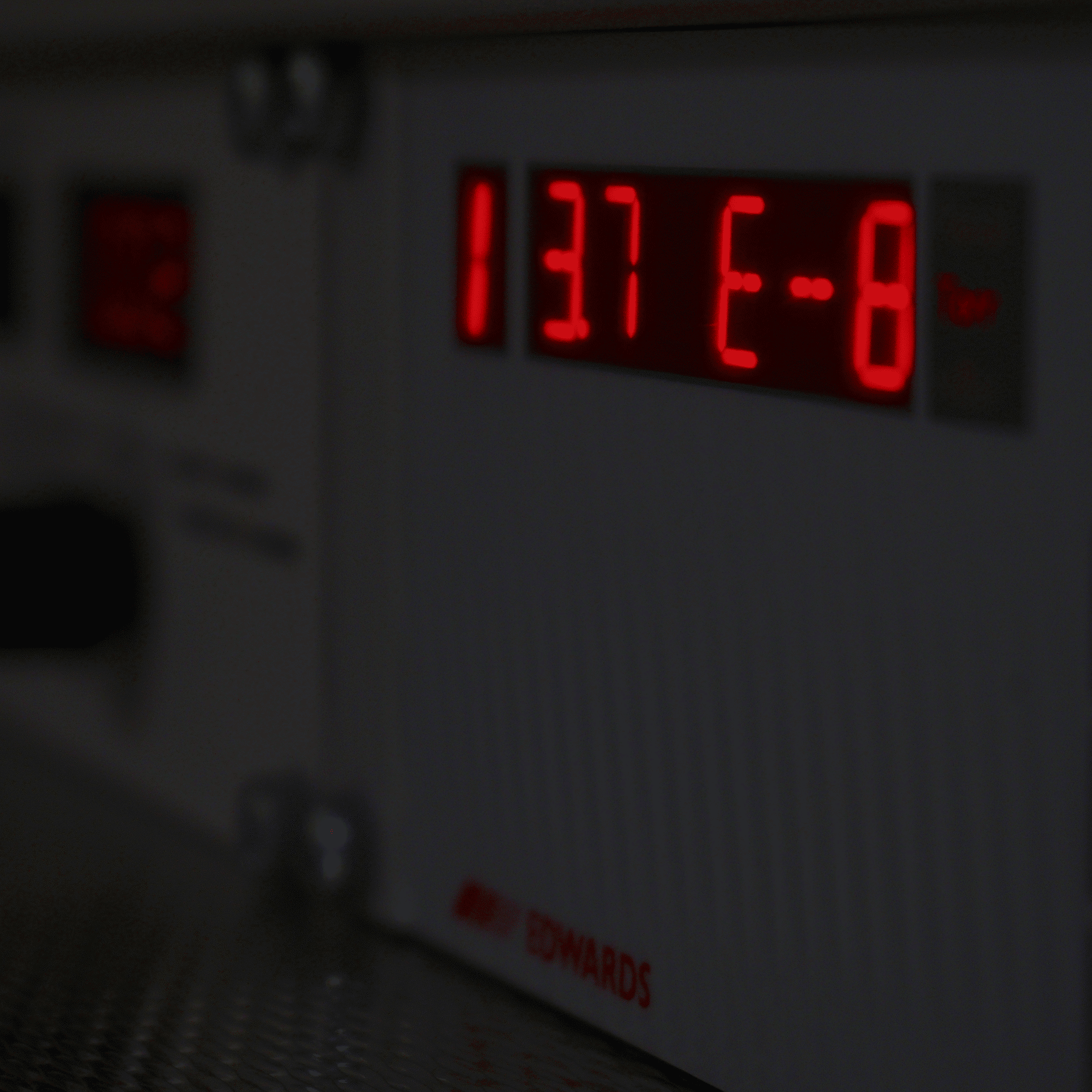
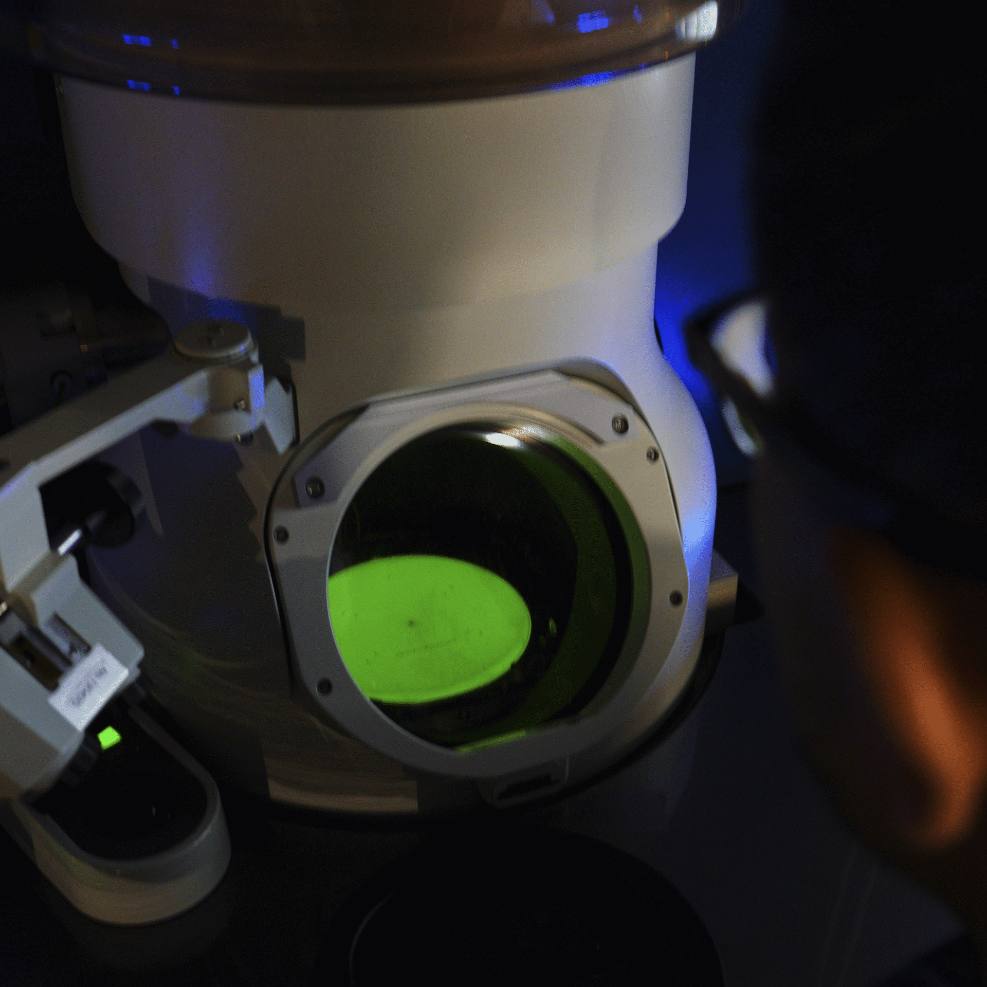
Optical Emission Interferometry (OEI) in the Plasma-Therm Versaline PECVD
2024-09-03
Using endpoint detection in PECVD recipes to improve film thickness accuracy
Fabrication | Featured | News
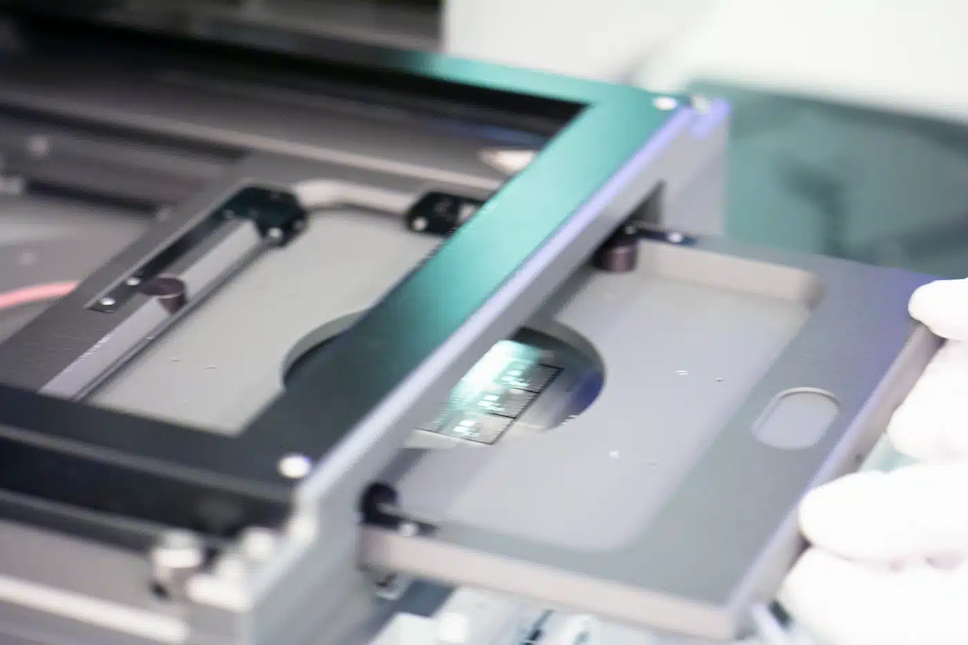
New Die Matrix Expander Available
2024-10-30
Improve your dicing post-processing with our new die matrix expander
Fabrication | Featured | News
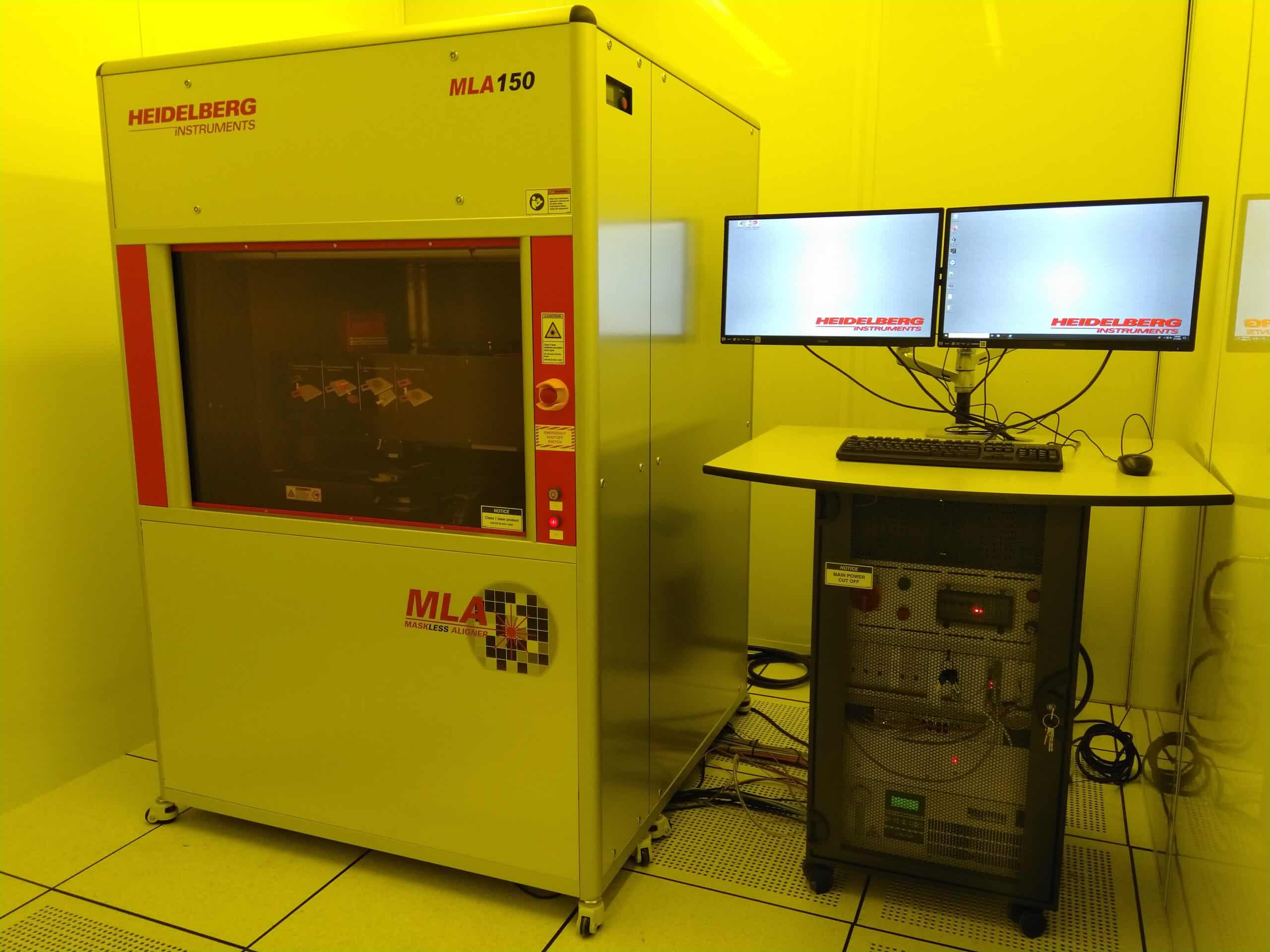
Field alignment now available on the Heidelberg MLA150
2025-10-23
Improve your DWL alignment precision with new field alignment capability

Totaling over $110 million in
specialized equipment and infrastructure
specialized equipment and infrastructure
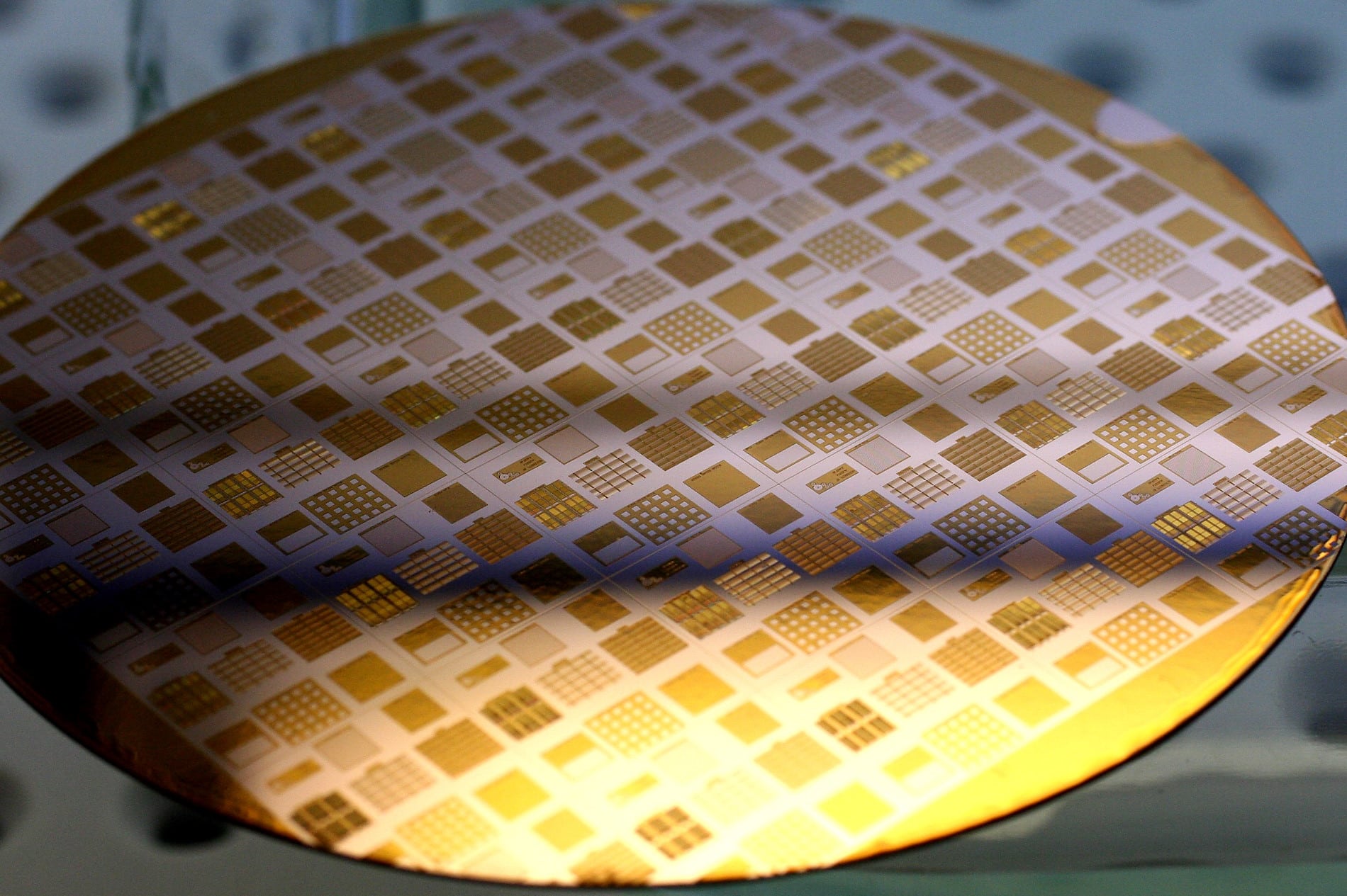
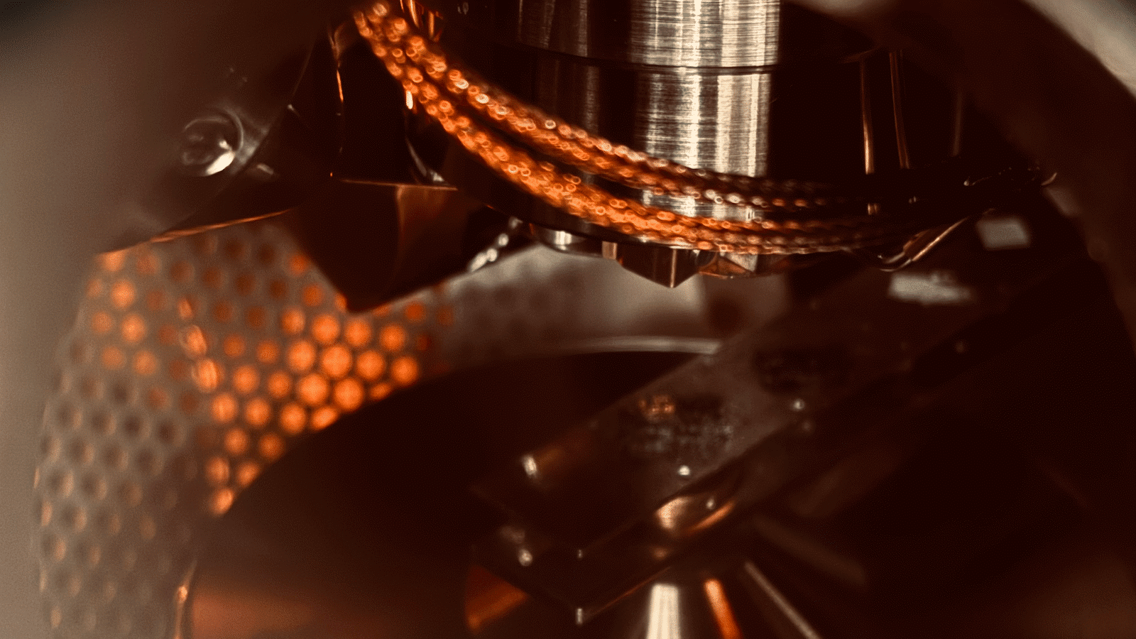
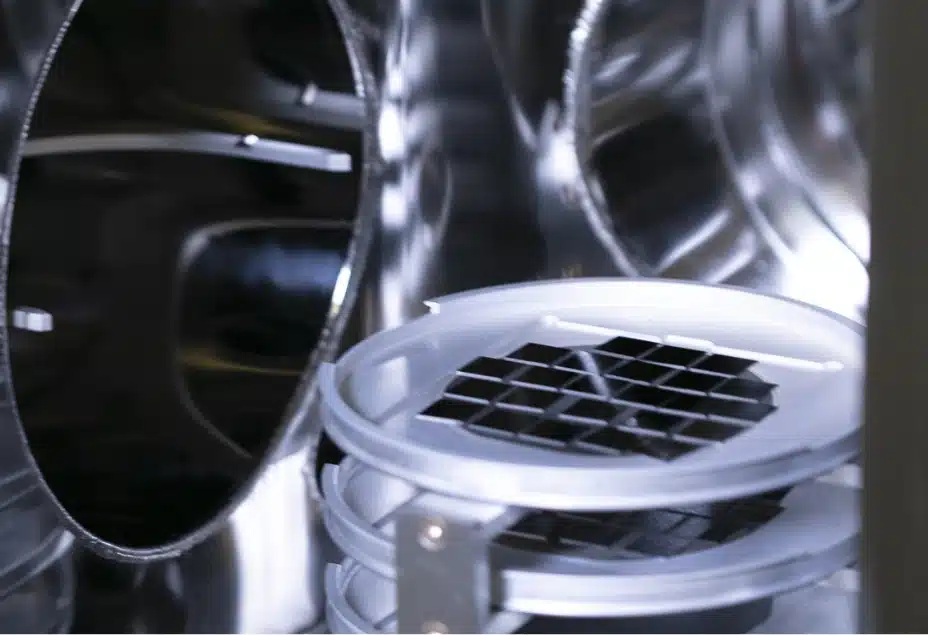
Fabrication for MEMS, sensors, microfluidics, and photonics
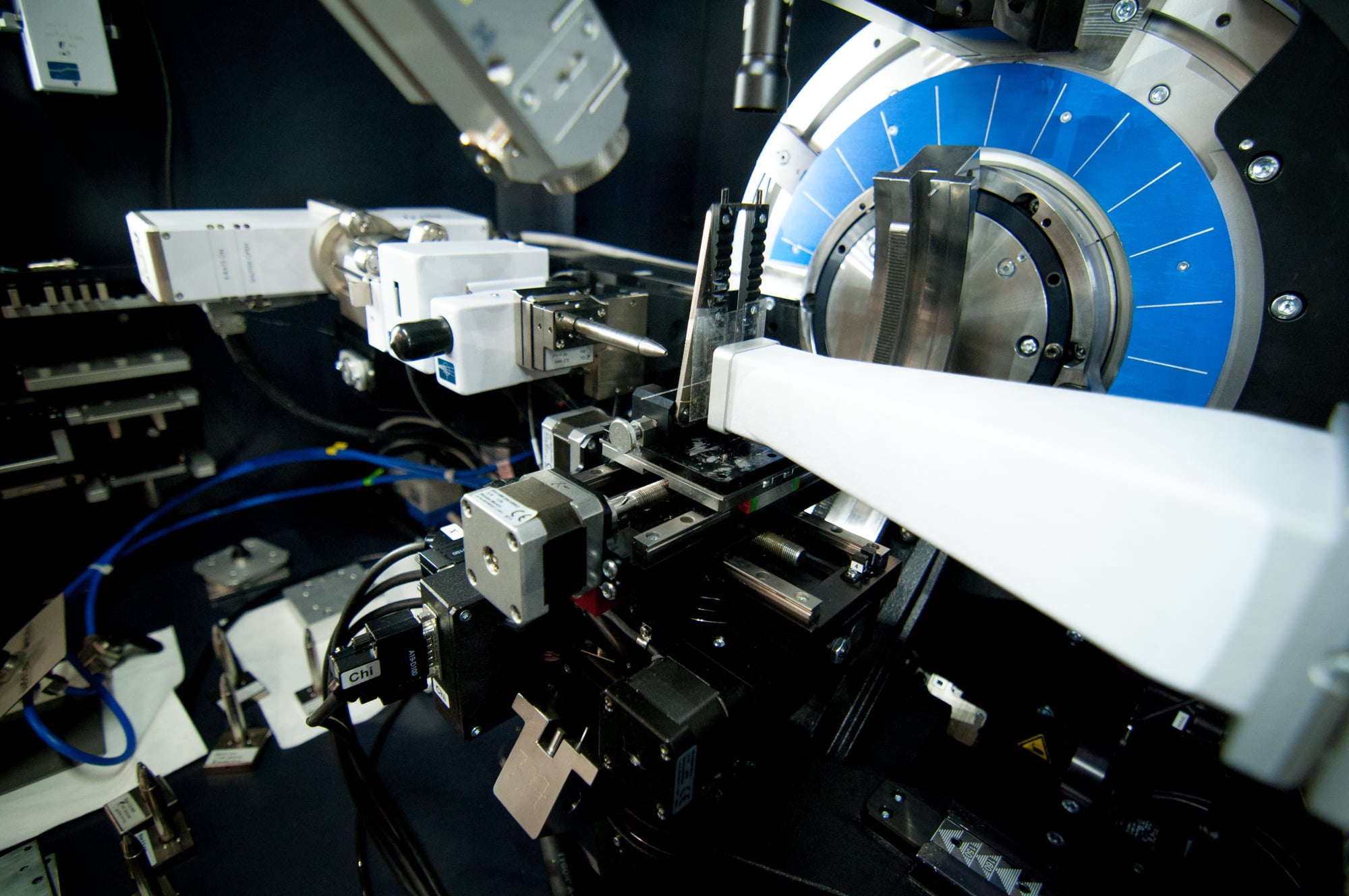
Advanced materials, microscopy, and spectroscopy analysis suite
Comprehensive capabilities for microscopy, spectroscopy, material analysis, lithography, thin-film deposition, and etching
Over 200 pieces of equipment in 25,000ft² communal laboratory space
Fully equipped 4" (100 mm) and 6" (150 mm) processing capabilities
We are an unparalleled Canadian centre supporting research and development in nano sciences and engineering.
Sign up
How to sign up
Objectives
Hands on training of academic and industry highly qualified personnel.
Process development and fee for service offerings for enhanced capabilities to support advanced research and industry development.
Support academic and industry development through proof of concept, prototyping and low volume manufacturing capabilities
Sustainable and transparent operations and administration

Facility Highlights
103465

Annual equipment-hours
175

Active tools
512

Active users
227

Active groups
Testimonials
Avalon Holographics has been an industrial user of the nanoFAB facilities for over 7 years. Having access to an open access shared cleanroom environment including a wide variety of microfabrication and characterization equipment has been instrumental to our process development and technology realization. Interactions with nanoFAB staff are friendly and professional, and their technical expertise serves as an excellent resource for problem solving and troubleshooting. We look forward to continuing to work with the nanoFAB in years to come!
Steve Rutledge, Ph. D.
Managing Director, Avalon Holographics
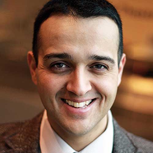
The nanoFAB is unique. It’s probably the best nanotechnology centre in western Canada. This is a facility that Canadians, Albertans, Edmontonians should be proud of. This is a facility that is going to build our future, and has been a big part of building diversified economies in Alberta for the past 15, 20 years. This is the future.
Hooman Hosseinkhannazer
CEO, Norcada

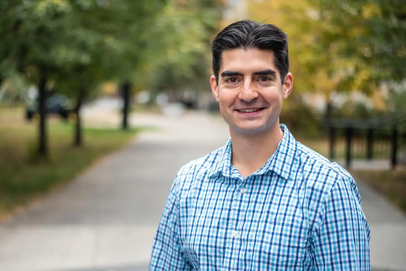
The nanoFAB is my second favourite place on campus, after my own lab. It basically has to be because nothing that we do in my lab could happen without the nanoFAB . Everything that we study at some point in its creation goes through the nanoFAB.
Dr. Mark Freeman
Professor, Faculty of Science - Physics, University of Alberta
Partnerships