
Advanced TEM Sample Preparation
Focused Ion Beam (FIB) provides preparation of site-specific, high-quality S/TEM samples for a wide range of materials. Unlike the conventional Ga-FIB, which has slow milling rate, results in Ga damage/implantation, the ThermoFisher Helios Hydra Plasma FIB (equipped with multiple inert ion species - Xe and Ar) overcomes those unwanted effects and produces damage free TEM lamellas./
The latest technological innovations on the Hydra PFIB microscope, such as flexible control of micro-manipulator and stage, multi-precursor gas injection system (GIS), along with well integrated software solutions, enable fast and easy lamella preparation with high throughput for TEM analysis, less dependent on the operators’ experience.
Our Characterization team is pleased to announce that all advanced processing for TEM lamella preparation on the Hydra PFIB have been successfully commissioned, including:
- Low voltage Xe and Ar beams to produce damage free samples
- Micro-manipulator (EasyLift) with continuous axial rotation, enabling flexible pluckouts, such as 90-degree / inverted pluckouts for both cross-sectional and plan-view preparation.
- Multiple precursors for Gas Injection System (GIS): C, Pt, W, providing flexible capping films for materials with different hardness and backfilling for porous materials.
- Automatic Lamella Sample preparation: fully automatic site preparation and software-assisted pluckout and final polishing.
Our user groups have utilized those techniques to produce TEM samples for their characterization needs. If you are interested in preparing TEM lamellas on the Hydra PFIB system, user training and staff analysis are available. Please submit a request (training or sample type) with sample details on LMACS. If you have any questions, please feel free to contact Dr. Shihong Xu (shihongx@ualberta.ca) - PFIB, Xuehai Tan (xtan@ualberta.ca) - TEM or Peng Li (peng.li@ualberta.ca) – the Characterization Group Manager.
Standard Lamella Preparation
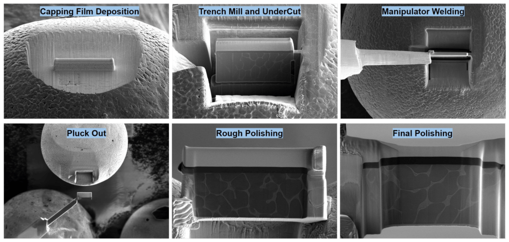
Application Examples
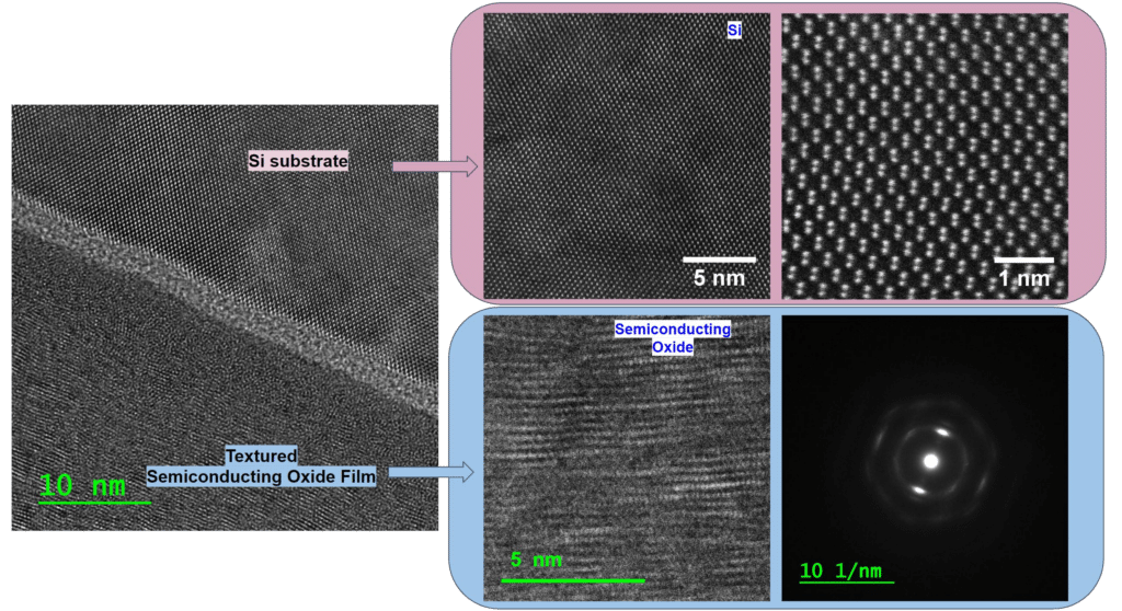
Sample: Semiconducting Oxide Film on Si
FIB Application: Low voltage 2kV Ar polishing to produce damage free sample for HR-STEM imaging
Sample Courtesy: Avalon Holographics Inc., Edmonton
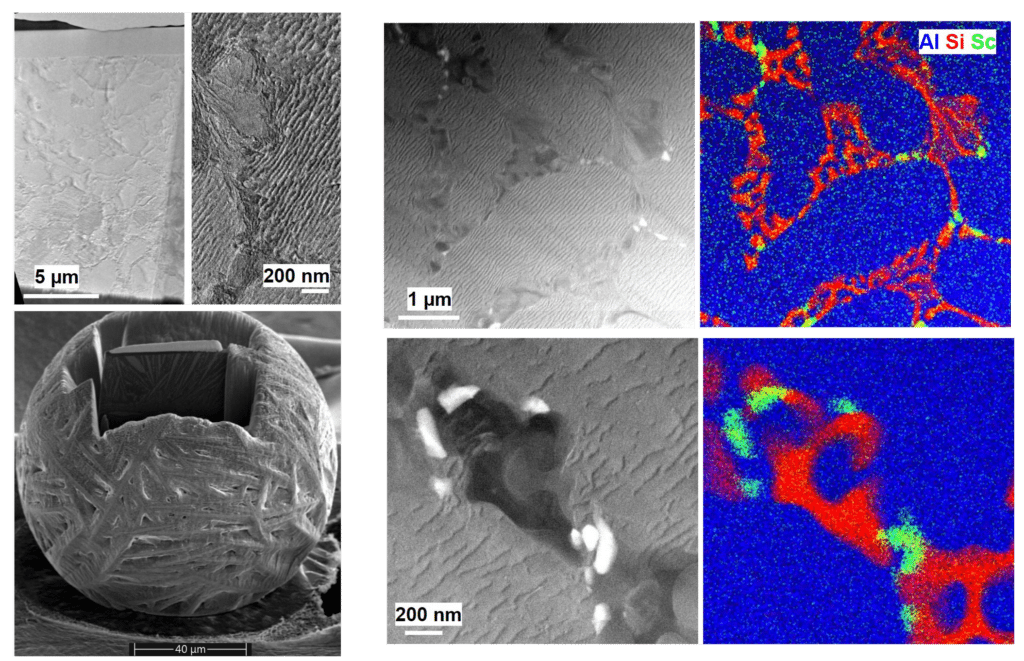
Sample: Rapidly solidified Al-10Si-0.4Sc droplets (atomized using Impulse Atomization)
FIB Application: Flexible micromanipulation to pluckout samples from spheres
Sample Courtesy: Akki Sahoo, Dr. Jonas Valloton and Prof. Hani Henein, Faculty of Engineering, University of Alberta; Abdoul-Aziz Bogno, Equispheres Inc., Ottawa
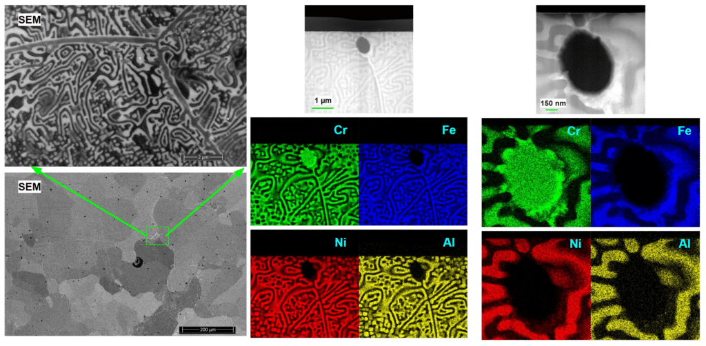
Sample: Al-Cr-Fe-Ni medium-entropy alloy (MEA)
FIB Application: Mixed Pt/C capping film for effective protection for HEA/MEA materials
Sample Courtesy: Guijiang Diao and Prof. Dongyang Li, Faculty of Engineering, University of Alberta
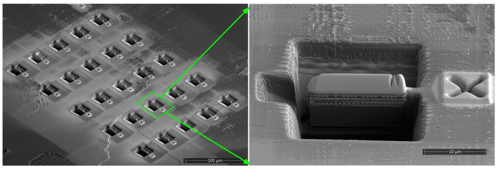
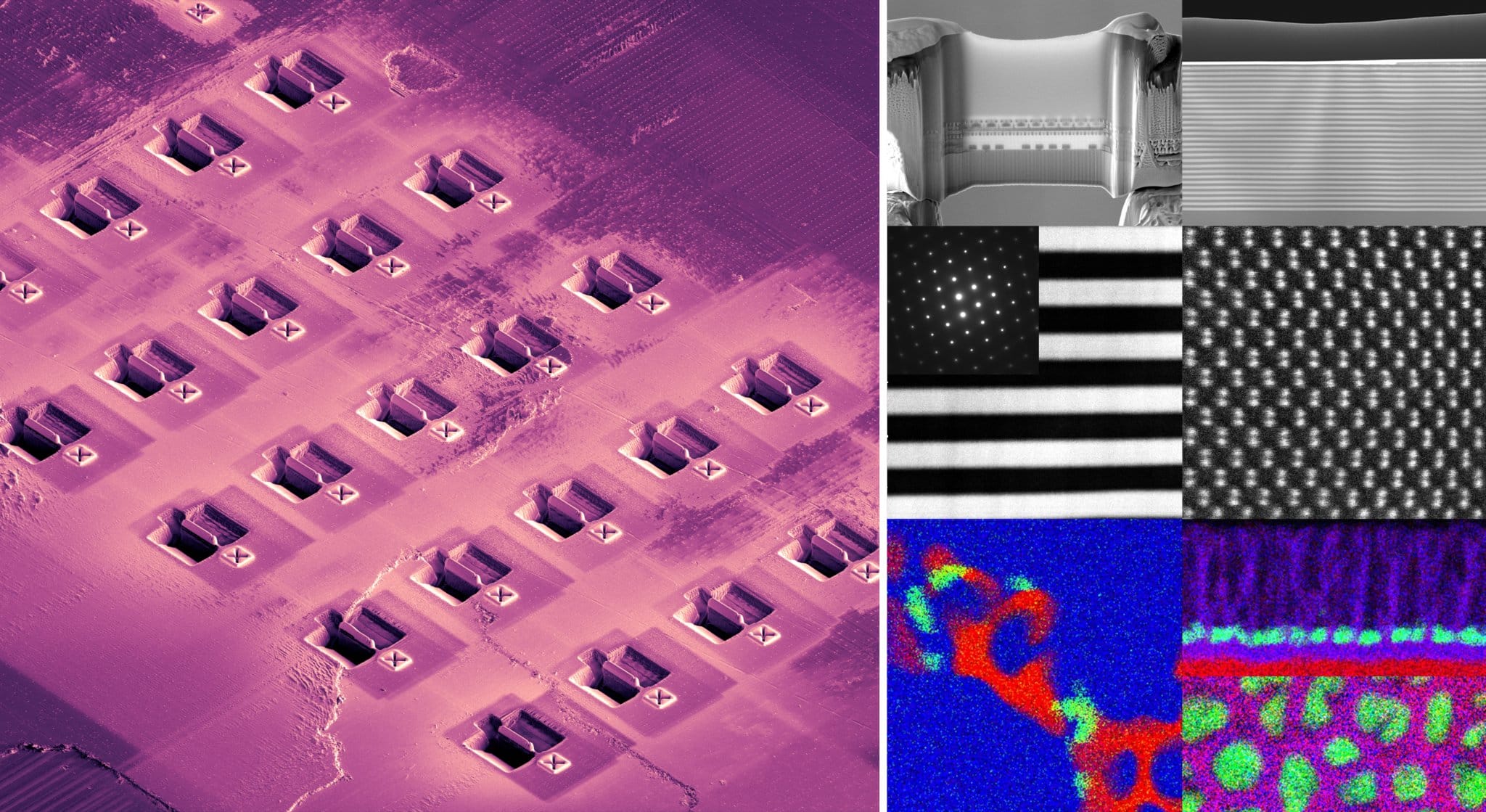
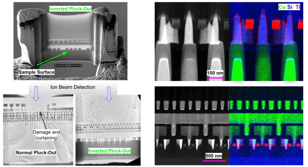
Sample: Intel Core i7 processor
FIB Application: Inverted pluckout to reduce curtaining and damage in the regions of interest.
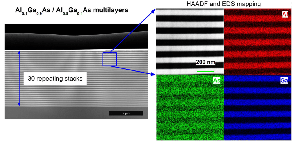
Sample: AlGaAs multilayers
FIB Application: 90-degree pluckout (ion beam parallel to the layer stacks) to produce uniform thin thickness across all layers.
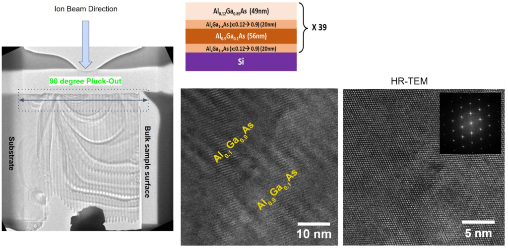
![Advanced TEM nanobeam diffraction images reveal crystallographic mismatch in Al[_x]Ga[_{1-x}]As/Al[_y]Ga[_{1-y}]As layers, complemented by a selected area electron diffraction pattern.](https://www.nanofab.ualberta.ca/wp-content/uploads/2025/02/06b-Al-Ga-As-1024x410.png)
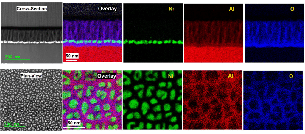
Sample: Nano-composite material (Ni nanoparticles in anodized Al)
FIB Application: Flexible miro-manipulation to produce cross-sectional and plan-view lamellas
Sample Courtesy: Dr. Matthew Nickel and Prof. Todd McMullen, Faculty of Medicine & Dentistry, University of Alberta
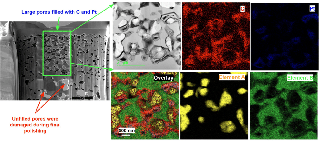
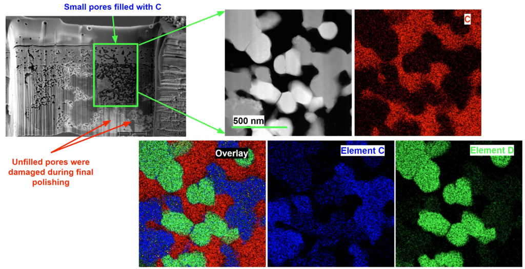
Sample: Porous solid oxide fuel cell
FIB Application: Back-filling with in-situ GIS to prepare high quality samples from porous materials.
Sample Courtesy: Prof. Douglas Ivey, Faculty of Engineering, University of Alberta
Sample: Intel Core i7 processor
FIB Application: Fully automatic/unattended site preparation of 25 locations