

Multilevel deep etching in silicon
Deep reactive ion etching (DRIE) of Si is a core process in MEMS and other Si micromachining applications. The cyclic Bosch etch process enables deep (tens to hundreds of µm), high-aspect-ratio features to be etched in Si, with vertical sidewalls, fast etch rates (>10 µm/min), and high selectivity to both photoresist (~100:1) and oxide (~300:1).
However, when fabricating multilevel designs—wafers which have two or more different etch depths, differing by some tens of µm—the deep features enabled by DRIE can pose a challenge. A common application requiring multilevel designs is microfluidics, where PDMS is cast and cured in a mould fabricated from a Si wafer: multiple etch depths are needed to produce channels with different flow characteristics, or to introduce constrictions between channels.
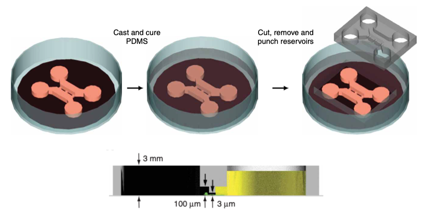
Example of multilevel PDMS microfluidics device.[Ref 1, Ref 2]
Although <1 µm of photoresist thickness is required to mask a 20 µm deep etch, spin-coating such thin photoresist over a 20 µm feature can yield poor resist uniformity. Depending on the lateral feature sizes in the design, there can also be challenges in exposing resist at the bottom of a trench (e.g., proximity exposure in a mask aligner, depth of focus in a direct-write system). These effects combined can frustrate efforts to faithfully reproduce the desired design features on the wafer—a problem which is only exacerbated as the number of levels increases.
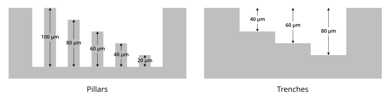
One method to overcome these challenges is to take advantage of the large selectivity afforded by a thermal oxide mask when Bosch etching: by building up a multilevel hard mask in the SiO2 prior to performing any DRIE, the maximum topography variation is that of the oxide thickness only, such that conventional spin-coating of thin photoresist and exposure can proceed without difficulty. To illustrate this process, we used a design consisting of five pillar heights and three trench depths, to be etched in a Si wafer:
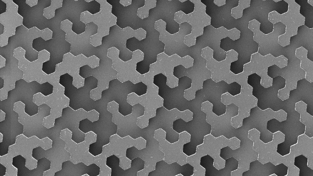
The lateral design consists of an Escheresque tessellation of unit cells with 3-fold rotation symmetry, purely for visual appeal.
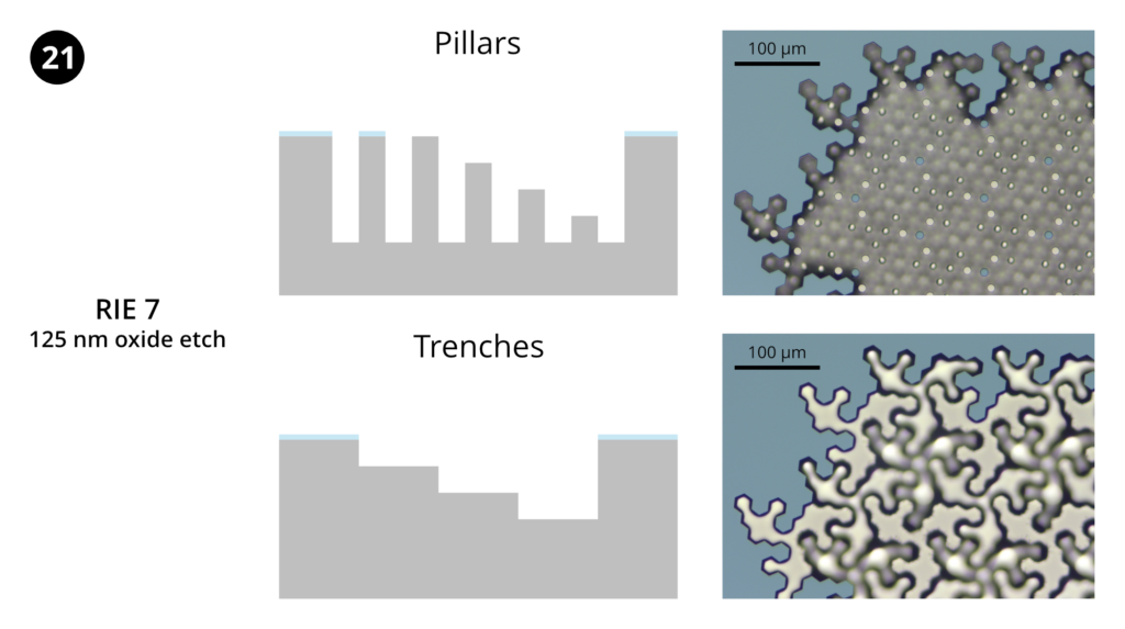
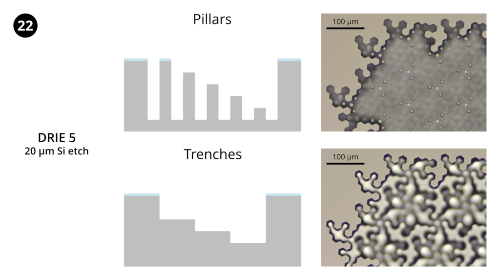
Process flow
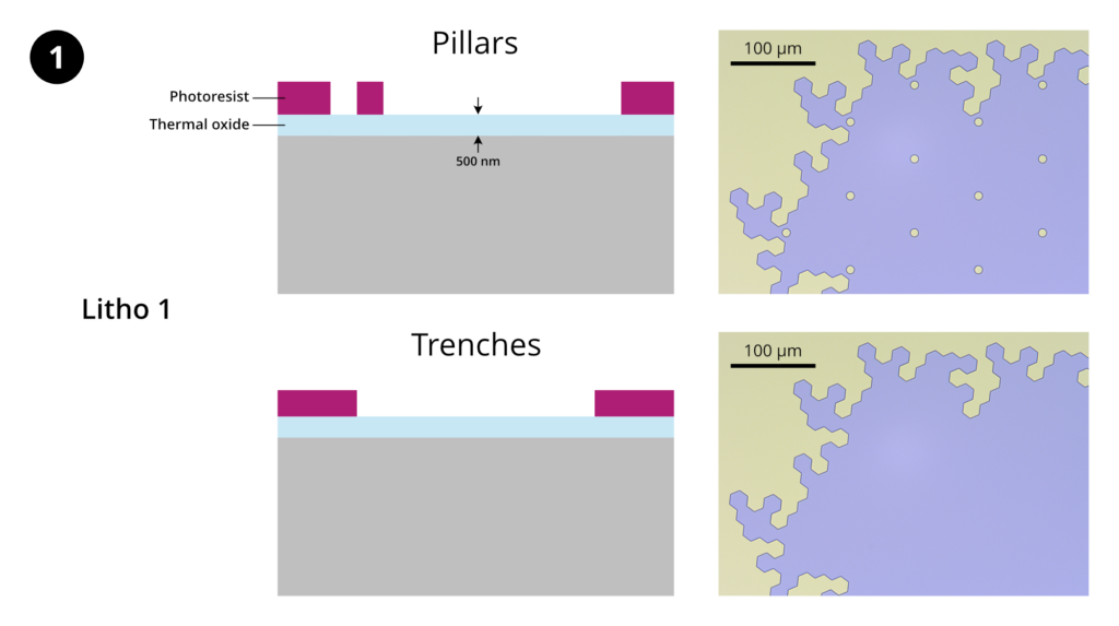
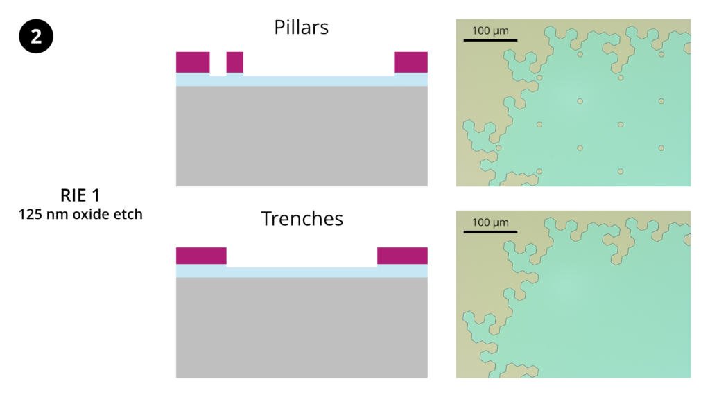
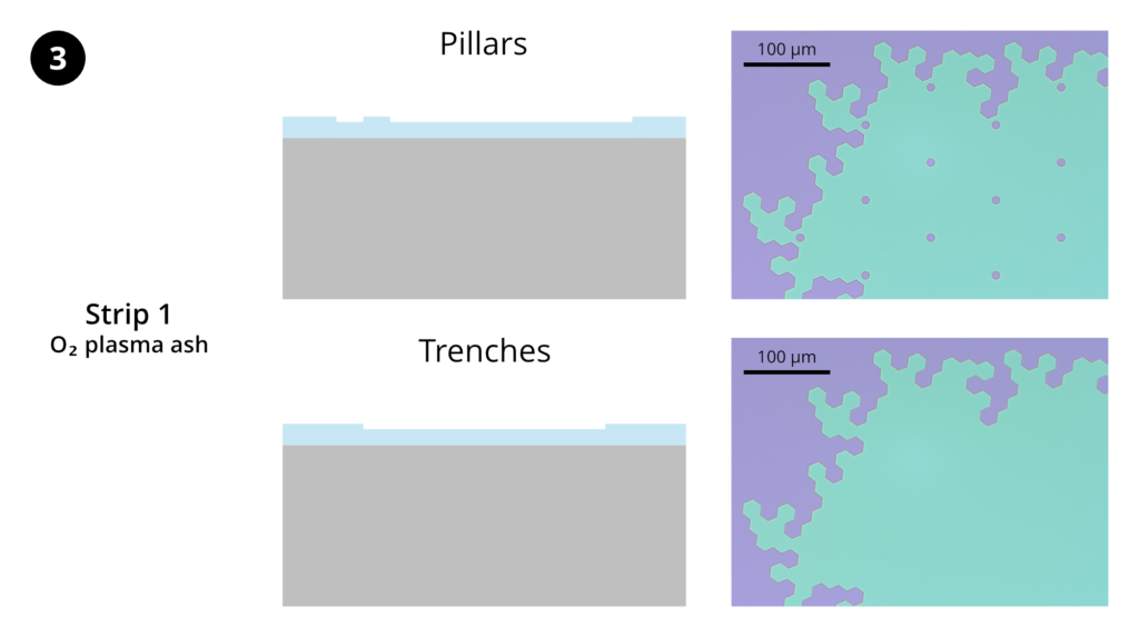
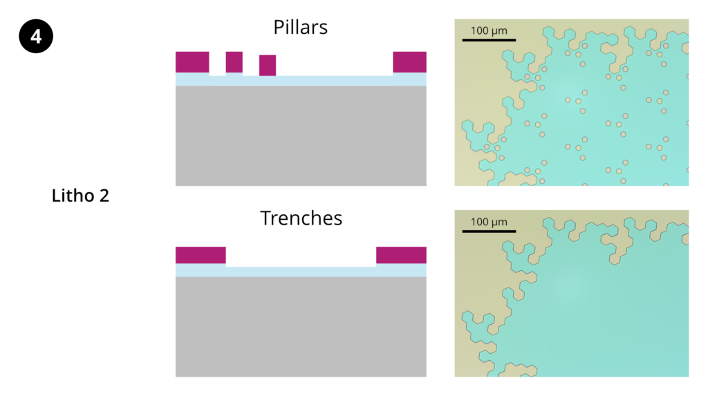
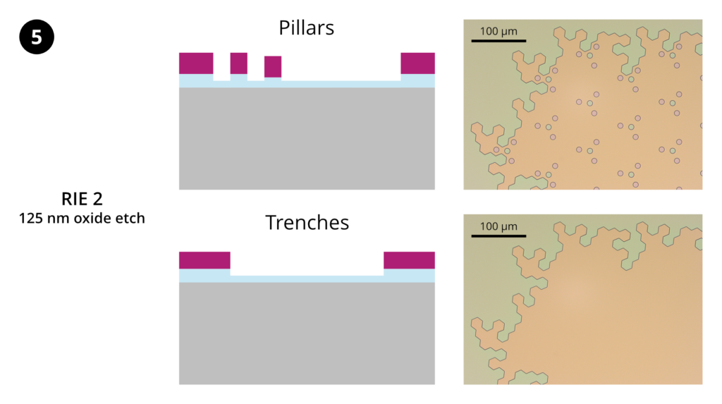
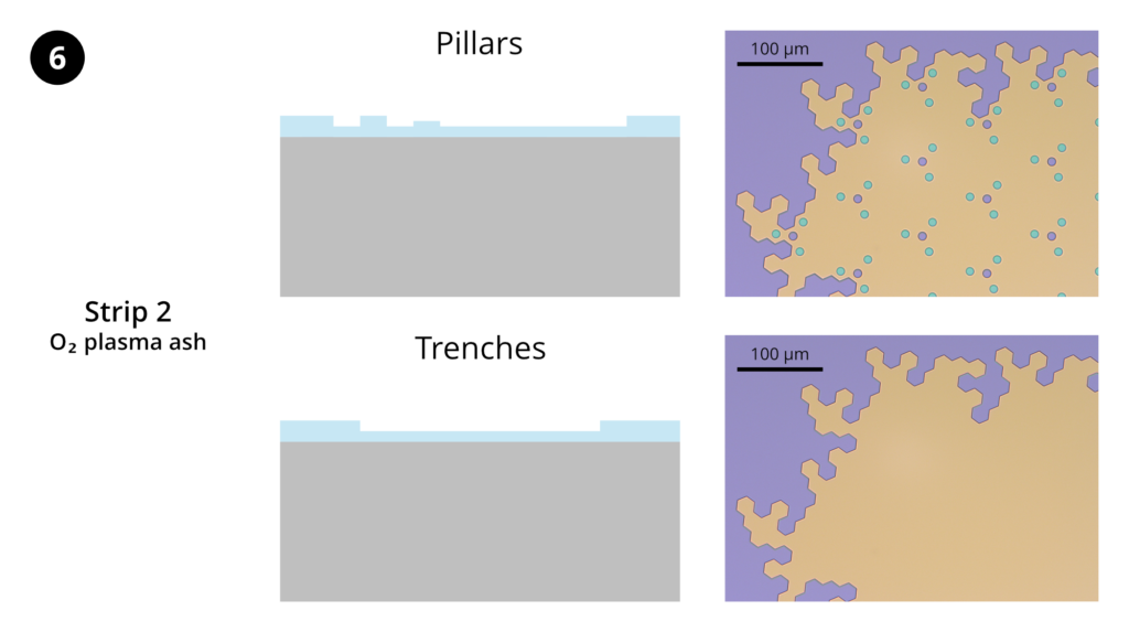
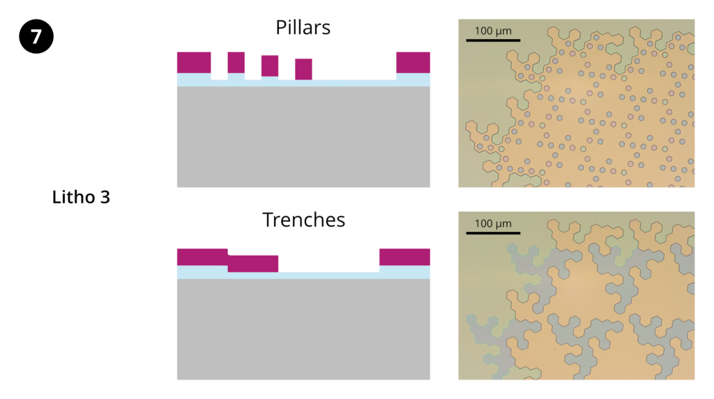
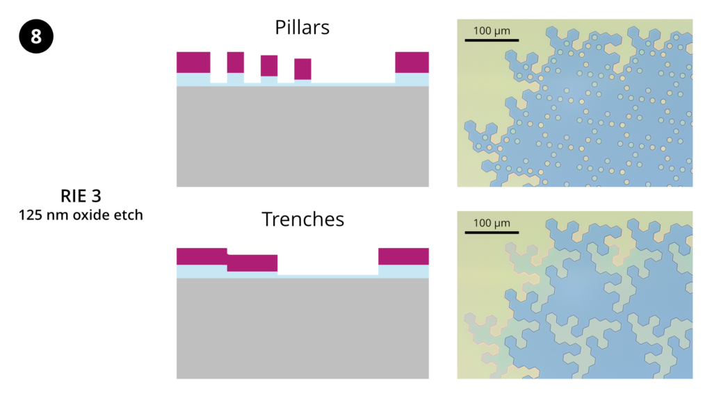
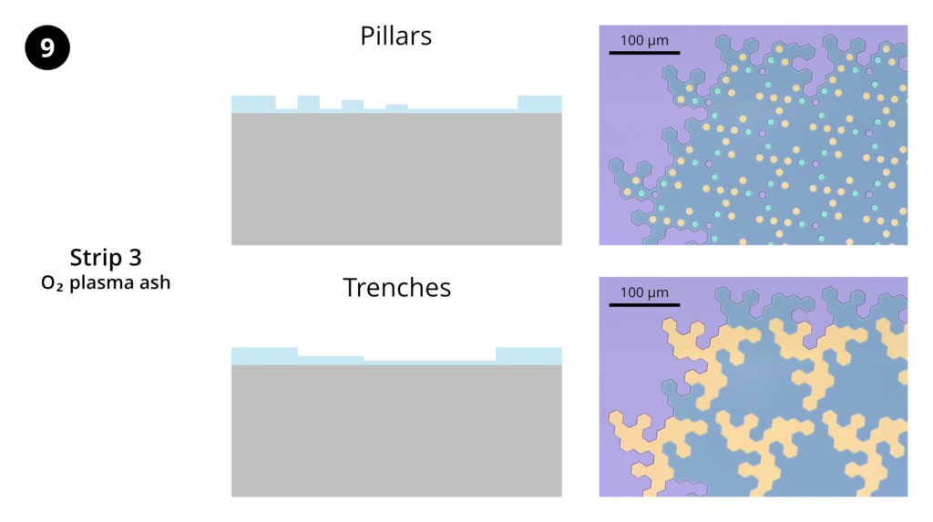
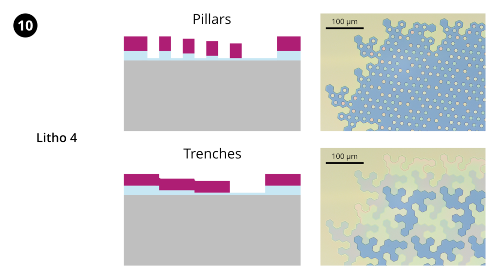
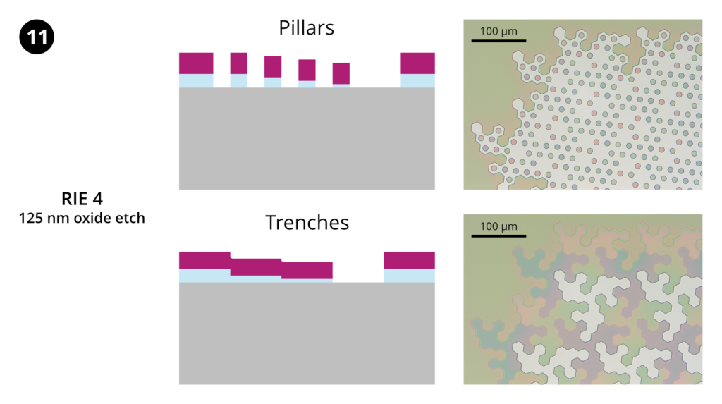
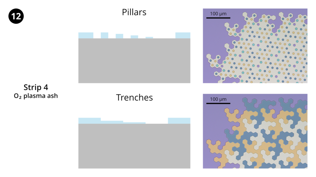
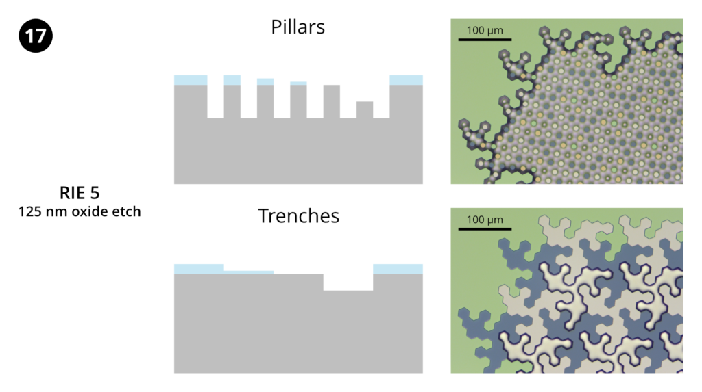
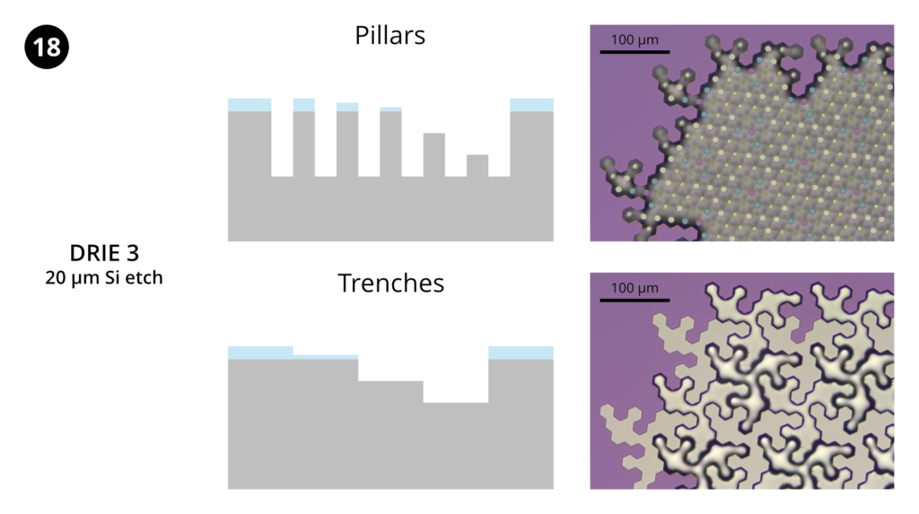
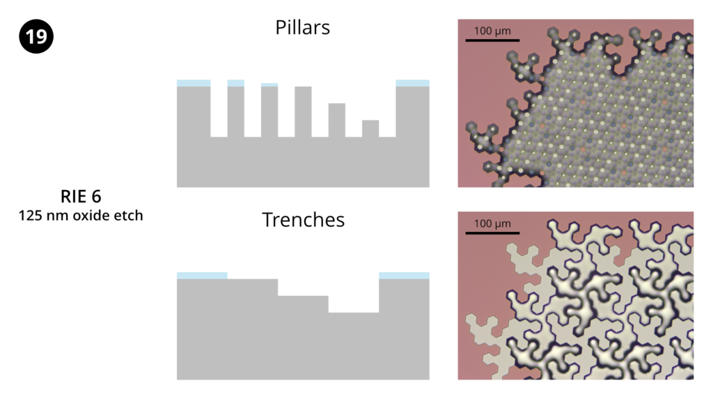
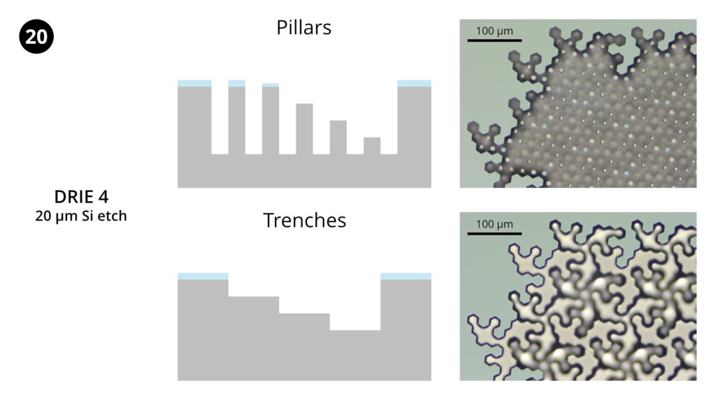
In the following process flow, the substrate is a standard 525 µm thick, 100 mm diameter Si prime wafer with ~500 nm of thermal oxide; ~1.1 µm of AZ 1512 was used for the photoresist, and exposures were done using the Heidelberg MLA150 direct-write laser lithography (maskless aligner) system. The resist strip and oxide etch steps were performed on the Trion RIE, and the DRIE steps were done using the “Bosch smooth sidewall” etch on the Oxford Estrelas ICPRIE. Cross-sectional diagrams (not to scale) of the pillar and trench structures are shown on the left; the right column shows optical microscopy images after performing the given process step.
Step 1: Lithography 1
Step 2: Reactive ion etching 1
Step 3: Resist strip 1
Step 4: Lithography 2
Step 5: Reactive ion etching 2
Step 6: Resist strip 2
Step 7: Lithography 3
Step 8: Reactive ion etching 3
Step 9: Resist strip 3
Step 10: Lithography 4
Step 11: Reactive ion etching 4
Step 12: Resist strip 4
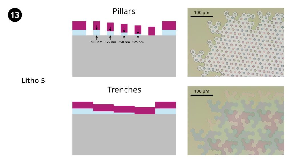
Step 13: Lithography 5
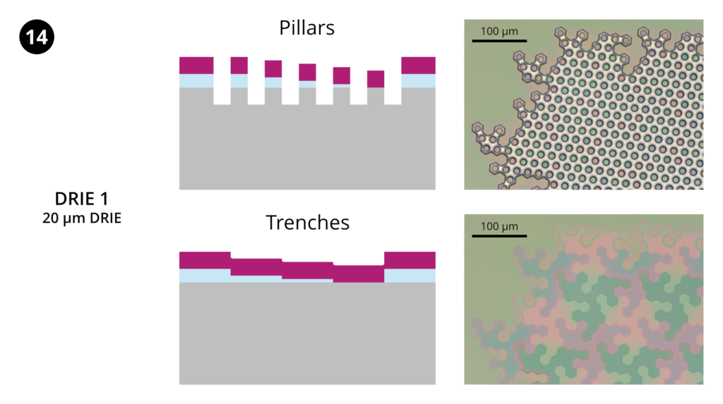
Step 14: Deep Si etch 1
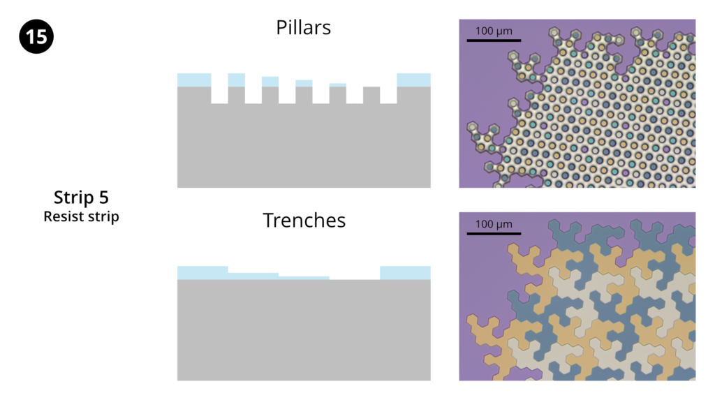
Step 15: Resist strip 5
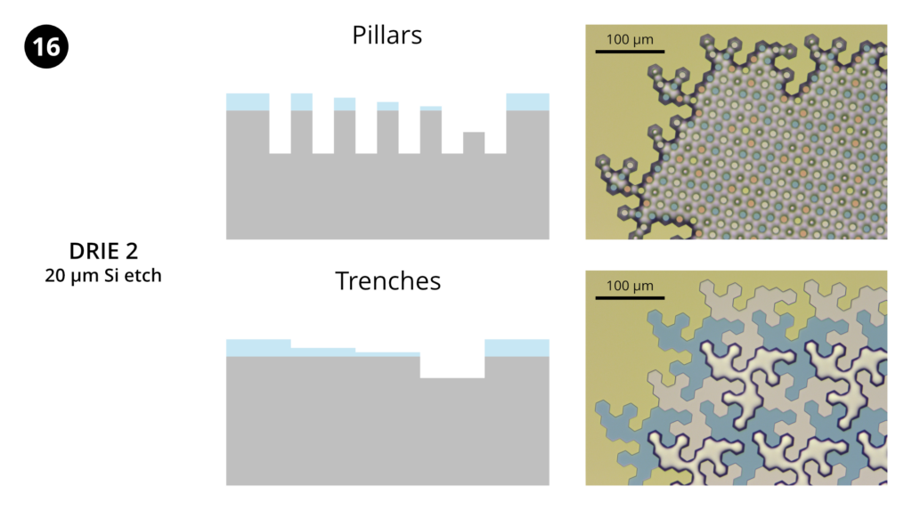
Step 16: Deep Si etch 2
Step 17: Reactive ion etching 5
Step 18: Deep Si etch 3
Step 19: Reactive ion etching 6
Step 20: Deep Si etch 4
Step 21: Reactive ion etching 7
Step 22: Deep Si etch 5
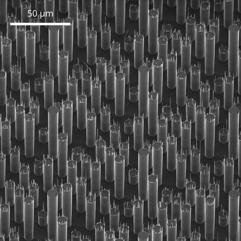
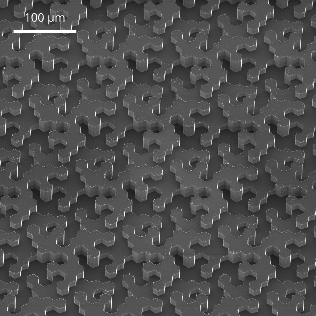
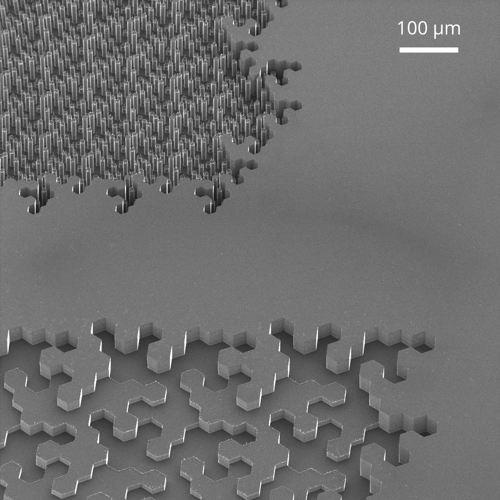
Imaging the final structures using He ion microscopy (HiM), both the pillars and trenches look as expected: adjacent features with heights differing by tens of µm are well formed, with vertical sidewalls and flat horizontal surfaces (pillar tops and trench bottoms). Note that many features are ringed with spikes of Bosch fluoropolymer residue—this specimen could benefit from further cleaning as described in our Bosch polymer removal comparison news post.
Pillars (40° tilt)
Trenches (40° tilt)
Pillars and trenches (40° tilt)
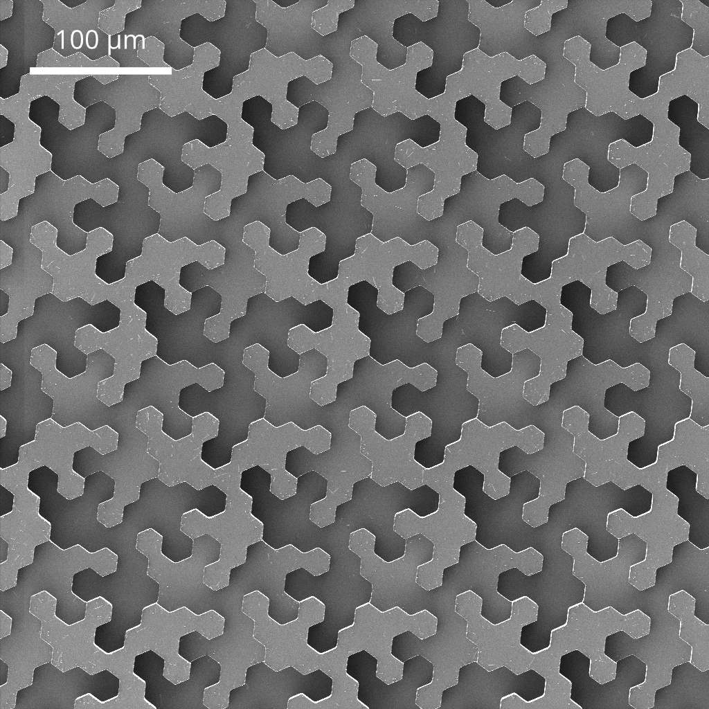
Trenches (0° tilt)
Application examples
We have applied the above multilevel DRIE technique two recent fee-for-service fabrication projects in the microfluidics application space, both involving Si moulds for PDMS casting.
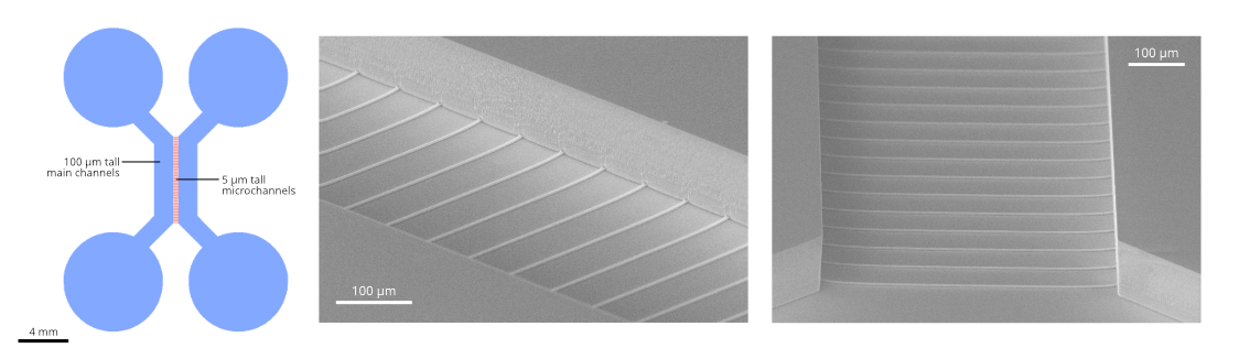
Microfluidic device layout (left), and SEM images (middle, right) of two-level Si mould. Two 100 µm tall main channels are connected at the bottom by 5 µm tall microchannels.
Courtesy of Shaun Sanders group (U Guelph).
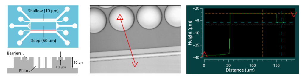
Microfluidic device layout and Si mould cross-section (left), and 3D optical profilometry scan (middle, right) of two-level Si mould. 10 µm deep barrier structures restrict flow into a 50 µm tall pillar array region.
Courtesy of Anne Benneker group (U Calgary)
For more information about using this technique in your own fabrication work, or for fee-for-service fabrication enquiries, please contact Aaron Hryciw (ahryciw@ualberta.ca).