Back to Capabilities
Thin Film
Deposition
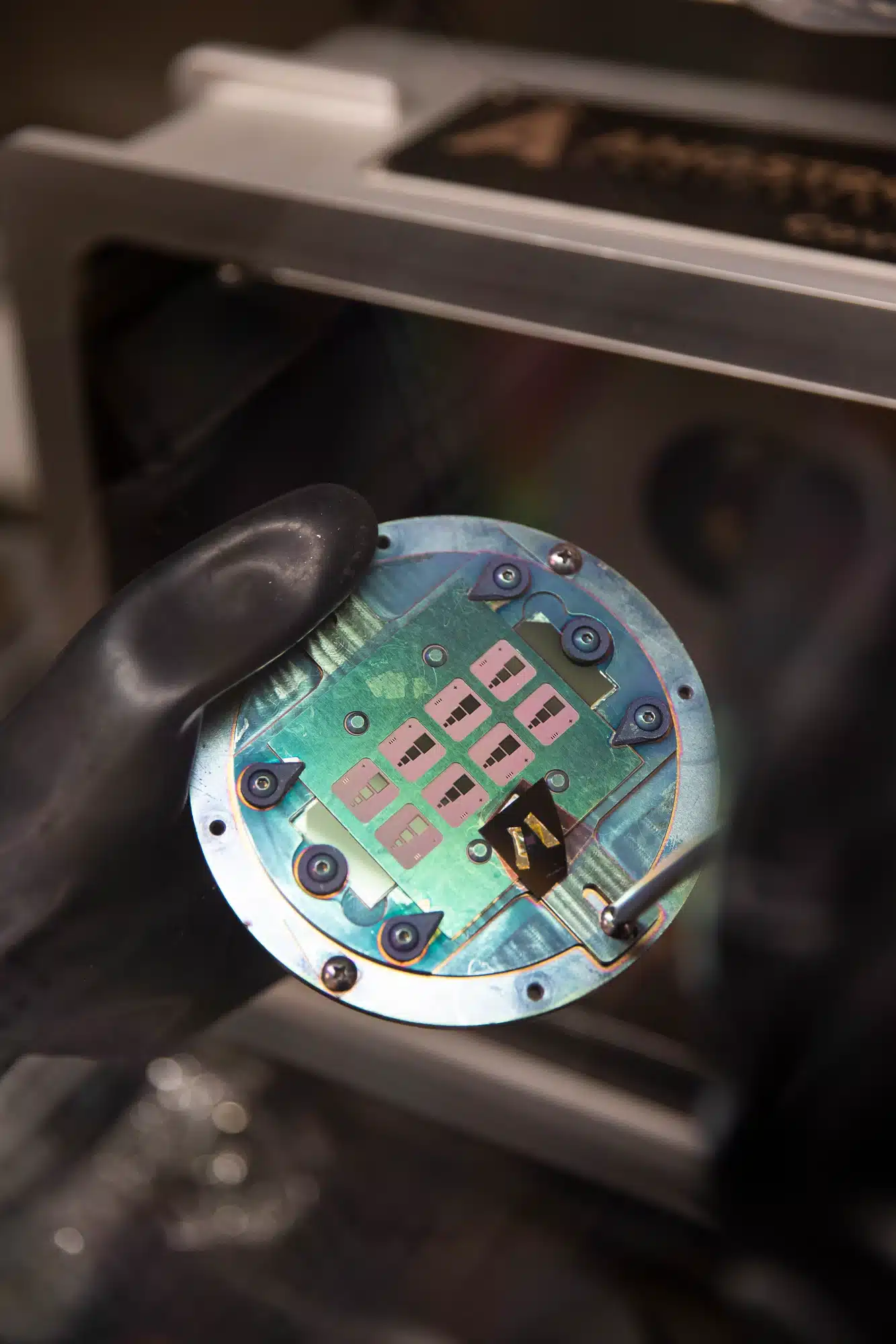
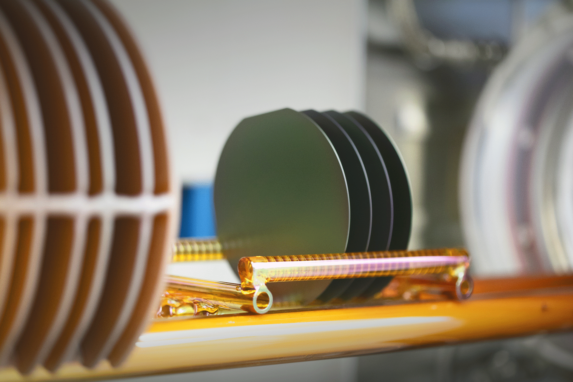
Deposition of metal, dielectric, and semiconductor thin films on substrates ranging from small chips to full 150 mm wafers. Capabilities include physical vapour deposition (PVD), chemical vapour deposition (CVD), and atomic layer deposition (ALD), enabling precise control over film composition, thickness, stress, and uniformity.
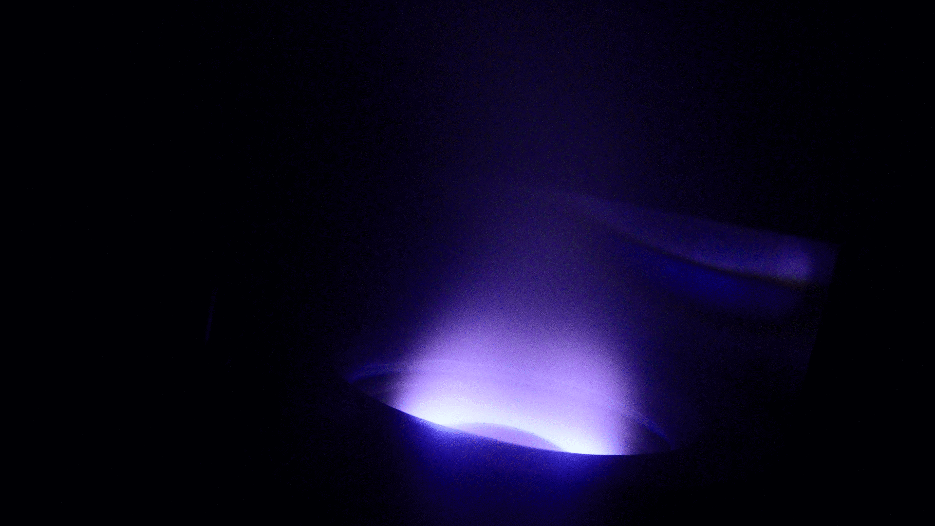
Magnetron sputtering
- Fully automated, loadlocked systems for high throughput and repeatability
- Manual, open-load systems for flexible processing (single- and multi-wafer)
- DC, pulsed DC, and RF power supplies
- Co- and reactive (O2/N2) sputtering
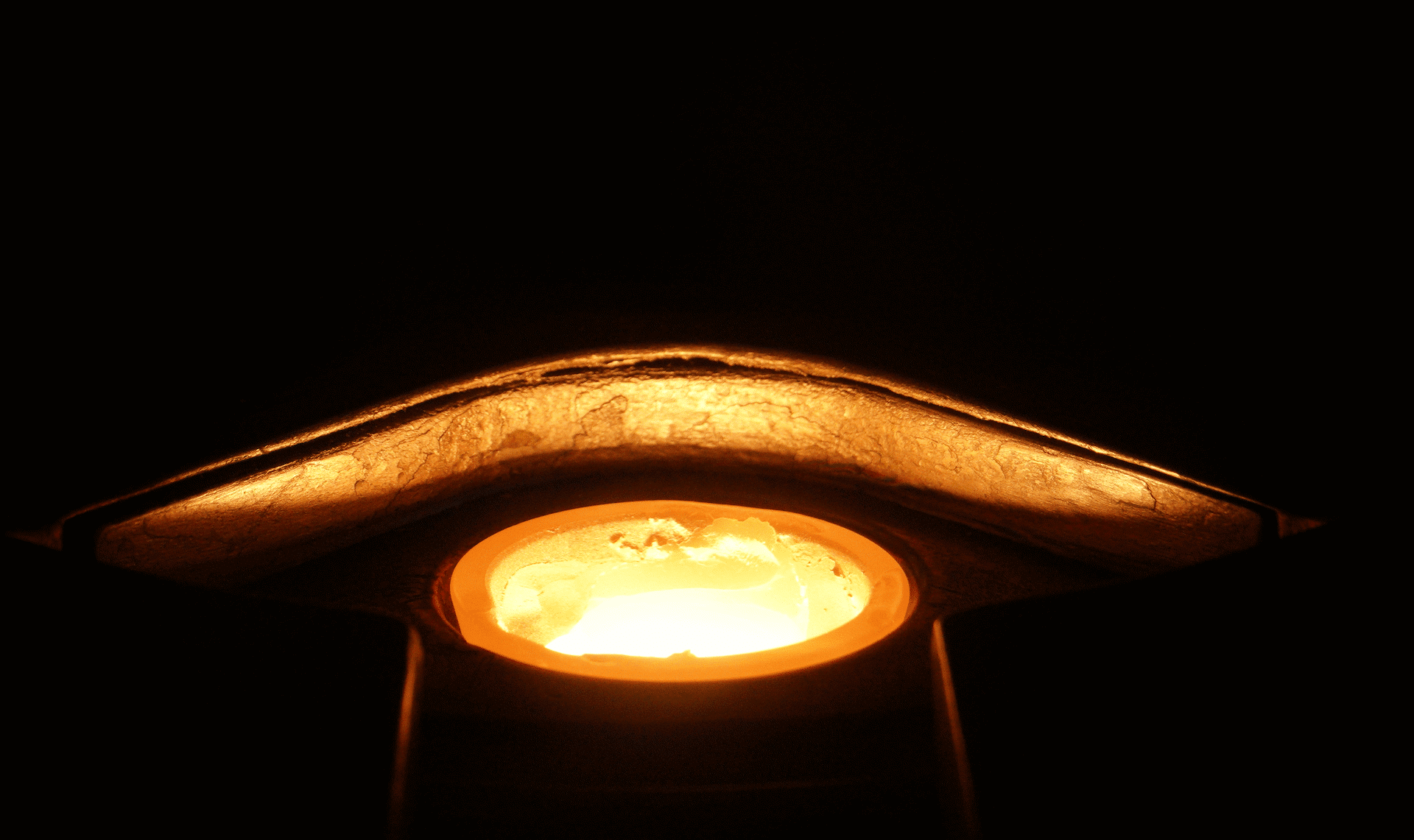
Electron-beam evaporation
- Fully automated and manual systems for deposition of metals and dielectrics
- Reactive (O2/N2) evaporation for oxides/nitrides
- Glancing-angle deposition (GLAD) system for nanostructured thin films (automated substrate tilt and rotation)
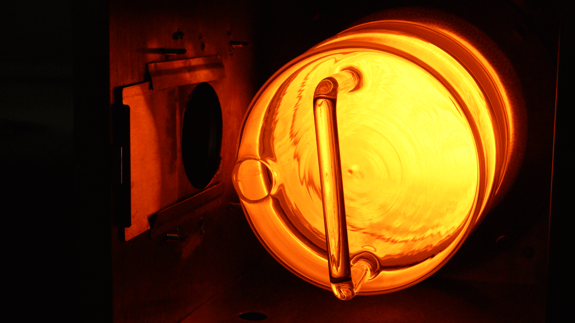
Thermal oxidation
- Wet and dry oxidation of Si for high-quality oxide growth (up to 50 wafers/batch)
- General-purpose annealing
- Rapid thermal processing/annealing
Low-pressure chemical vapour deposition
- Automated batch processing system (up to 50 wafers/batch)
- Deposition of low-stress nitride, stoichiometric nitride, amorphous Si, poly-Si, and boron-doped poly-Si
Plasma-enhanced chemical vapour deposition
- SiO2, SiOxNy, SiNx, and amorphous Si deposition
- Tunable stoichiometry and film stress
- Optical emission interferometry for process monitoring and endpoint detection
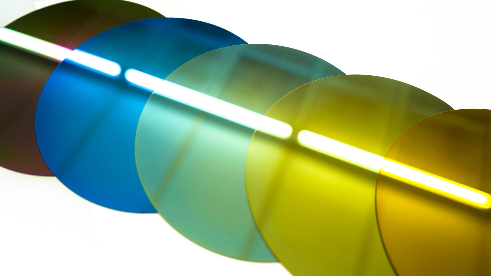
Atomic layer deposition (ALD)
- Thermal and plasma-enhanced ALD processes
- Highly conformal films with atomic-layer thickness precision
- Qualified recipes for oxides and nitrides of Al, Si, Ti, Zr, Hf, Pt
- In situ ellipsometry for process monitoring and endpoint
Thermal organic evaporation
- Four evaporation sources with independent quartz crystal microbalance thickness monitors
- Enclosed in glovebox for processing air-sensitive materials
- Dedicated OLED processing