Back to Capabilities
Advanced Lithography
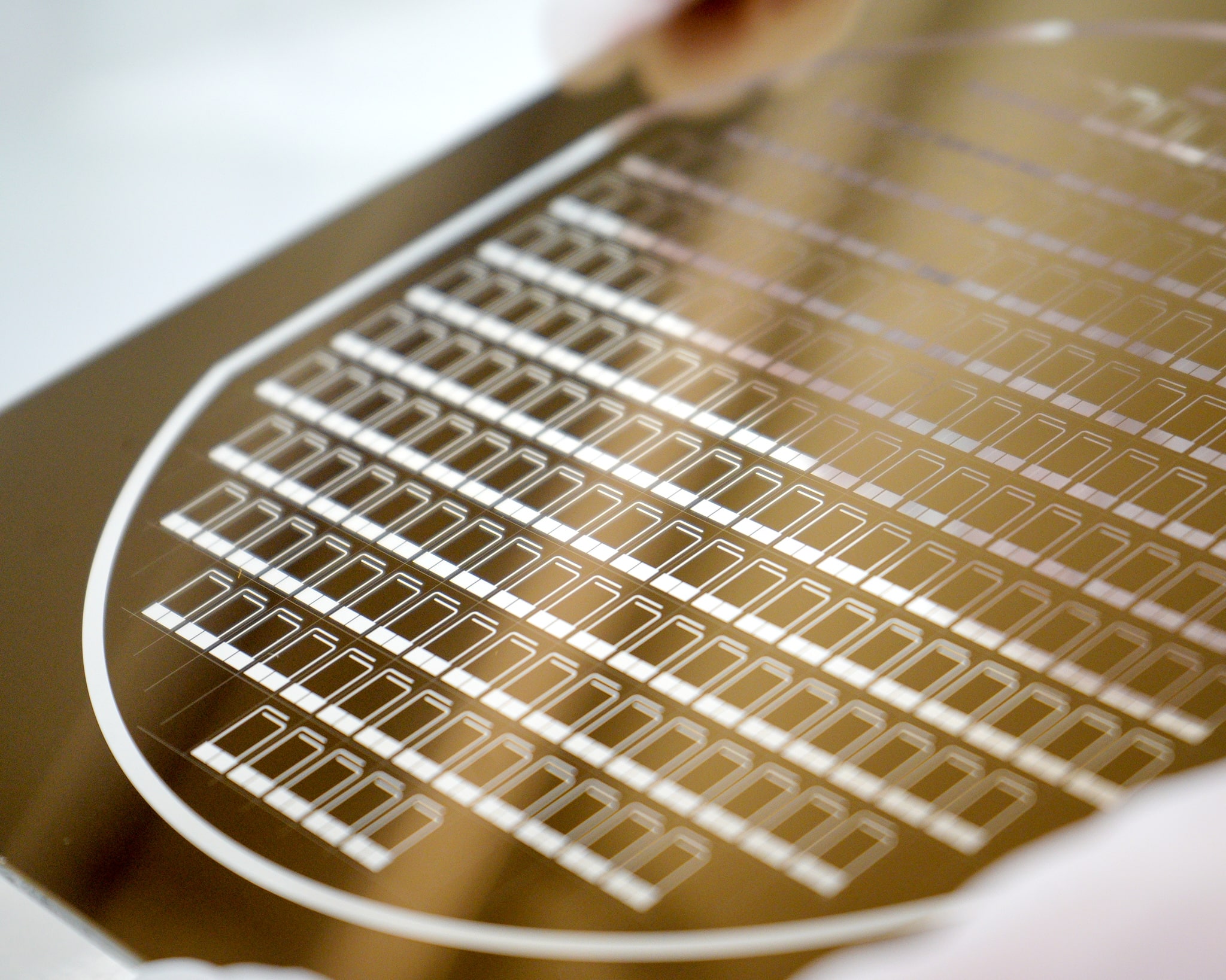
Precise micro- and nanoscale patterning is available through our suite of lithography tools, including electron-beam lithography (EBL), direct-write (maskless) laser lithography, two-photon polymerisation 3D printing, and conventional contact mask aligners.
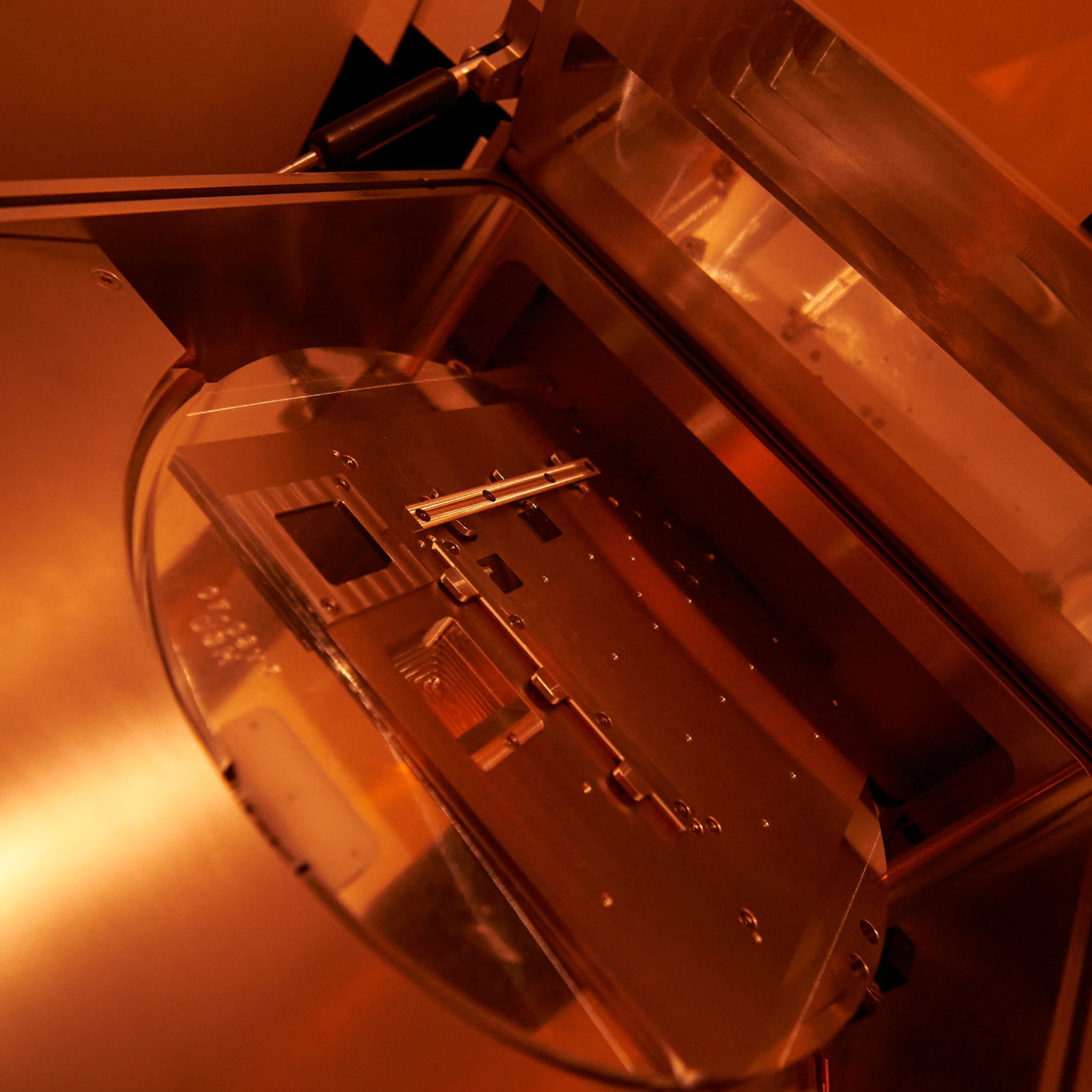
Direct-write laser lithography
- Heidelberg MLA150 maskless aligner
- Expose wafers directly from GDSII pattern file: no need for a photomask
- Automated topside and backside alignment
- 405 nm / 375 nm exposure
- High-aspect-ratio mode and greyscale lithography
Electron Beam Lithography
- RAITH Voyager (50 kV) and RAITH150 Two (0.2–30 kV) EBL systems
- Interferometric laser stage for stitching
- <10 nm minimum feature size
- FBMS/MBMS mode enables full-wafer, stitch-free processing
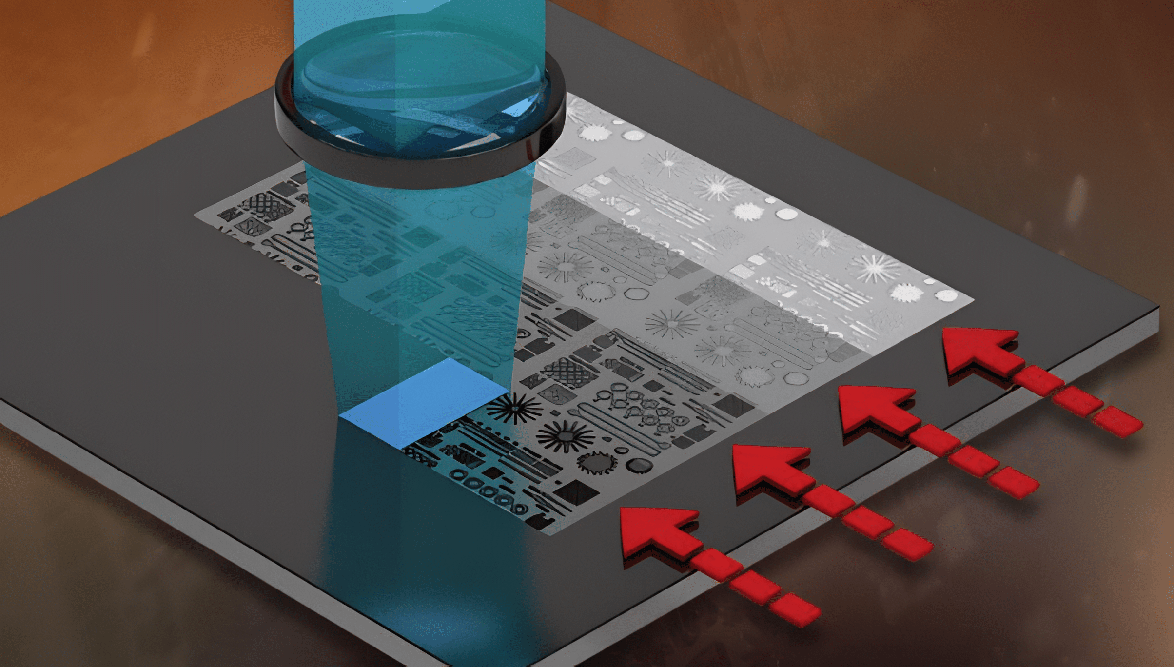
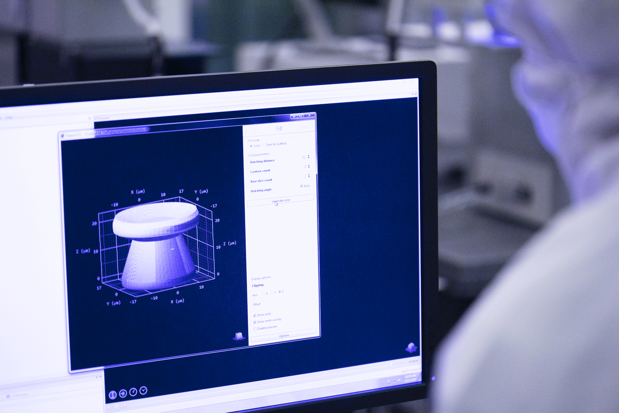
Nanoscale 3D Printing
- Two-photon polymerization process for microscale 3D printing
- Submicron feature sizes in all 3 axes
- Dynamic precision printing modes for a wide range of applications
Contact photolithography
- General-purpose UV exposures
- H-line (405 nm) / I-line (365 nm)
- IR/optical backside alignment
- Deep-UV exposures (220 nm / 254 nm)
- Semi-automated alignment
- Positive/negative tone resist chemistries
In-house photomask fabrication
- Heidelberg DWL200 pattern generator
- Produces 5" & 7" photomasks
- 1 µm minimum feature size
- Full-service processing with online mask submission