Back to Capabilities
Plasma Etch
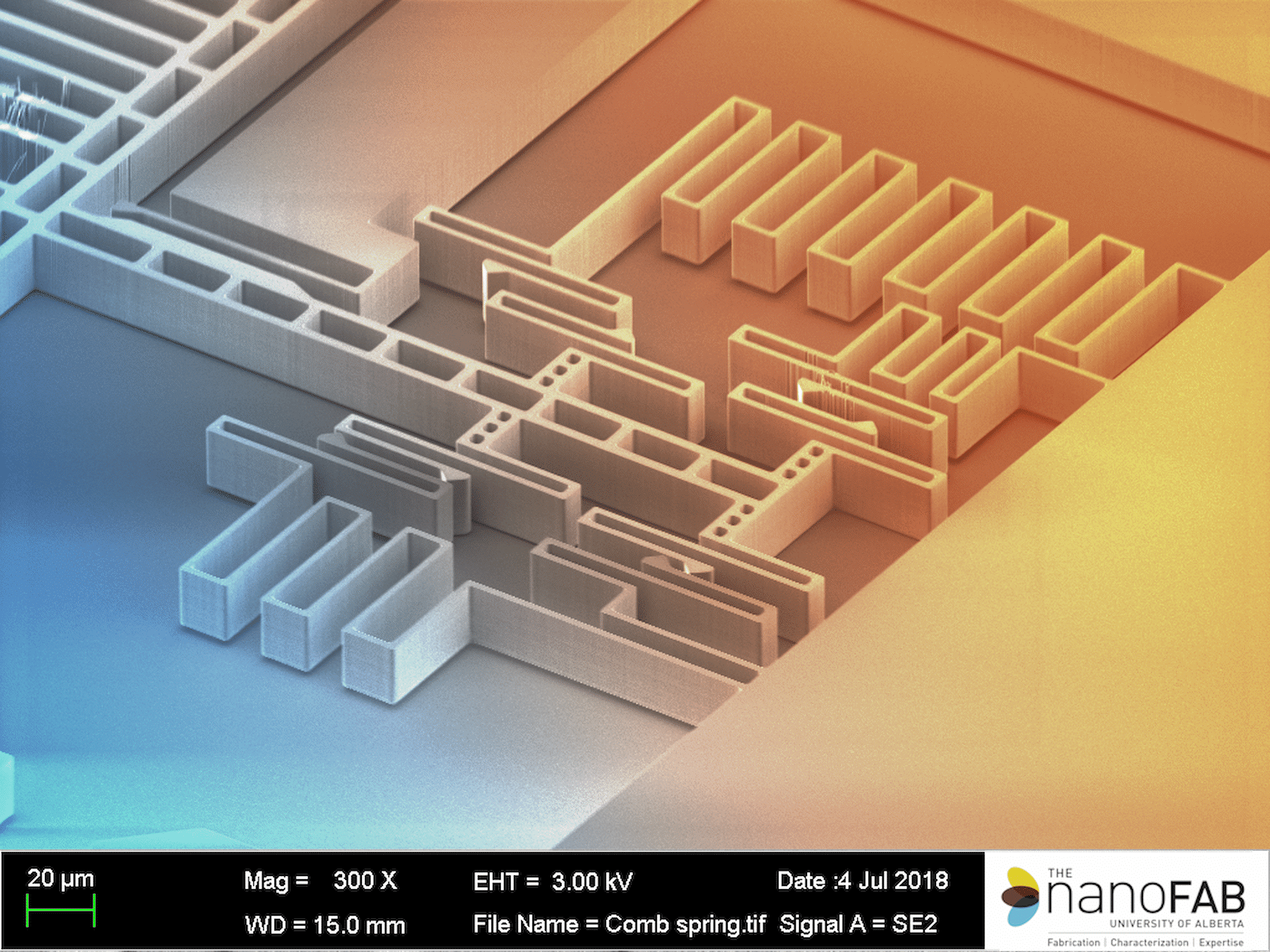
Plasma and dry etch processing provides exceptional control over etch depth, profile, and selectivity for a wide range of materials, supporting applications including microelectronics, photonics, and MEMS fabrication.
Deep reactive silicon etching
- Dedicated Bosch (DRIE) and cryo processing
- Nanometre scale to hundreds of µm (through-wafer) etching
- Sidewall profile and roughness control
- Plasma dicing for die singulation of arbitrary shapes and layouts
Reactive ion etching
- Dedicated SiO2, SiNx, and Si etching
- O2 plasma surface activation and polymer etching
- Plasma ashing for photoresist strip
Metal and III-V etching
- Dedicated etching for metals, compound semiconductors, and dielectrics
- Reactive and sputter-based etch recipes via ICPRIE
- Wide variety of process gases: Cl2, BCl3, HBr, SF6, CHF3, O2, Ar
- Backside He cooling
Vapour HF etching
- Dry oxide etch process for stiction-free release of MEMS devices
- Selectively etch different sacrificial oxides without attacking other layers
- Backside gas protection prevents etching oxide on wafer backside