

Advanced XPS Capabilities Are Available
While standard XPS/UPS analysis is available on the Kratos Ultra XPS, advanced capabilities provided by the PHI VP3 system are:
Imaging
The VP3 utilizes a raster scanned x-ray beam for imaging and probing applications. The X-ray beam induced secondary electron images (SXI) provide an easy of use workflow and precise sample positioning and navigation. The ultimate spatial resolution is determined by the X-ray probe size. A probe size as small as 7 μm can be routinely obtained. 10 μm Au squares (on Silicon) can be well revealed from both SXI images and Elemental Maps.
Depth Profile Analysis
The VP3 is equipped with two sputter guns for depth profile analysis: monatomic Argon (mono-Ar) ion gun and Argon Gas Cluster Ion Beam (GCIB). While the low energy mono-Ar gun provides excellent sputtering for inorganic materials (metals and semiconductors), the GCIB is designed to work with polymer and organic materials without causing chemical damages, thus providing access to quantitative chemical state information.
Depth profile analysis of a SiN/HfO2/SiN/HfO2 ALD film stacks on Silicon substrate by 2 kV mono-Ar ion gun. Each layer thickness = 20 nm:
Depth profile analysis of a MOSCAPs device, consisting of Ru (140 nm) / SiN (10 nm) / GaN (100 nm) on Silicon substrate, by 1 and 2 kV mono Ar ion gun:
Depth profile analysis of an OPV device, consisting of a polymer film stacks of P3HT:PCBM (250 nm) / PEDOT (30 nm) on ITO glass substrate: (1) overall C, S, O intensity profiles and (2) P3HT and PEDOT profiles based on different chemical states of S.
Sample Courtesy: Adrian Velazquez, Dr. Erik Luber and Prof. Jillian Buriak, Department of Chemistry, University of Alberta.
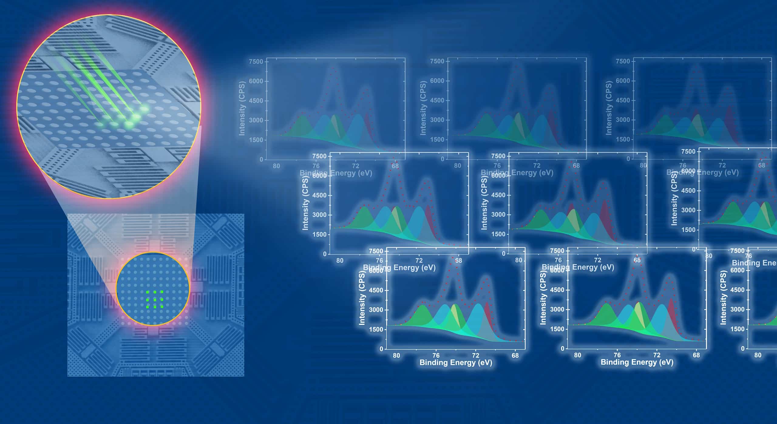
Automatic data acquisition
The Point Generation and Image Registration functions provide a solution of automatic data acquisition for high throughput analysis. Here is an example of XPS analysis of 100 Pt dots (60 μm in diameter) from an MEMS device, collected in 12 hours, with representative Pt 4f spectra from 10 (out of 100) locations and drift correction results.
Heating/cooling XPS
A hot/cold stage is available for XPS analysis in a temperature range from −140 °C to +600 °C. Preliminary heating XPS analysis was performed on a Si substrate as surface decontamination process. Hydrocarbon contamination on surfaces was significantly reduced at +600 °C. The surface remains clean when the sample is cooled down.
Angle Dependent XPS (ADXPS)
ADXPS is a non-destructive technique to analyze the thickness and composition of thin-film stacks with ultra thin thickness. Below are ADXPS results of Silicon with native oxide and Fluorine terminated Silicon surface. Hydrocarbon contamination on surfaces with a few Å in thickness was successfully revealed due to the high surface sensitivity of the technique.
ADXPS analysis of Si with native oxide
ADXPS analysis of fluorine terminated Silicon
The VP3 system is now open for sample analysis by staff and user training. Training is provided selectively to users who have projects that require regular XPS analysis after initial sample analysis by nanoFAB staff. Please submit a request on LMACS, if you are interested to submit samples for analysis or get trained on the tool. If you have any questions, please feel free to contact Peng Li (Peng.Li@ualberta.ca) – the Characterization Group Manager.