The nanoFAB is pleased to announce a new Applications/Research Specialist staff member – Dr. Nastaran (Nas) Yousefi in our Characterization group.
Nas is a physical/materials chemist with extensive research background in organic optoelectronic materials. During her PhD, she gained considerable experience with fabrication processes for organic electronics (e.g., transistors, biosensors), materials characterization (e.g., AFM, HIM, GIXAS), and electrical characterization techniques. Given the multidisciplinary nature of her research projects in the past, she has acquired a unique skillset that complements the expertise and capabilities at nanoFab.
Nas’ primary areas of responsibility are XRM, XRD/SAXS, BET, spectroscopy and electrical characterization/test tools. She will be working to support user training, fee-for-service work and process development. She is beyond excited to help researchers navigate through their path of discoveries and train students to become independent researchers.
Please join us in welcoming Nas!
Dr. Nas Yousefi in the Zeiss Xradia Versa 620 X-Ray Microscopy Lab
XPS analysis of air-sensitive materials
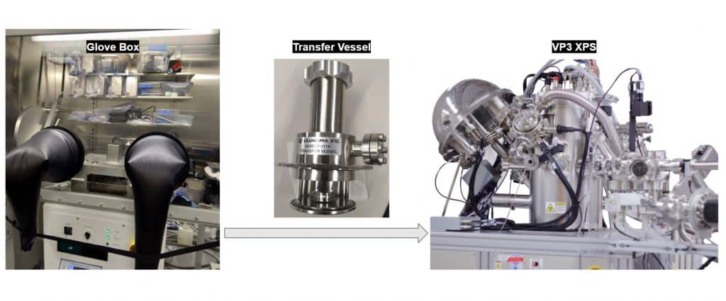
The nanoFAB is pleased to announce that analysis of air-sensitive materials is available on the PHI VP3 XPS system.
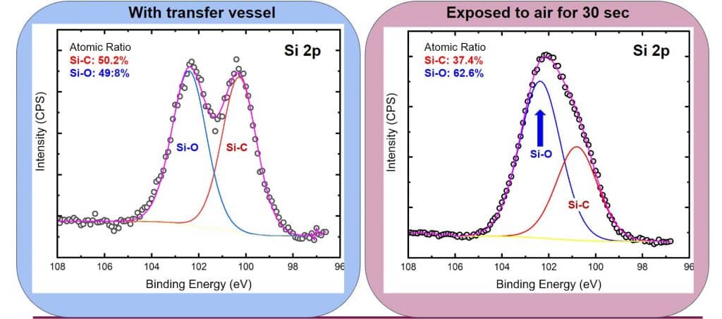
Proper sample handling is critical to analyze materials that are sensitive to air. We have been working to bring the capabilities of analyzing air-sensitive materials on to our analytical instruments. A controlled-environment transfer vessel is now commissioned and available to transfer samples from glove boxes to the PHI VP3 Versa Probe III XPS to minimize environmental exposure during sample transfer/loading.
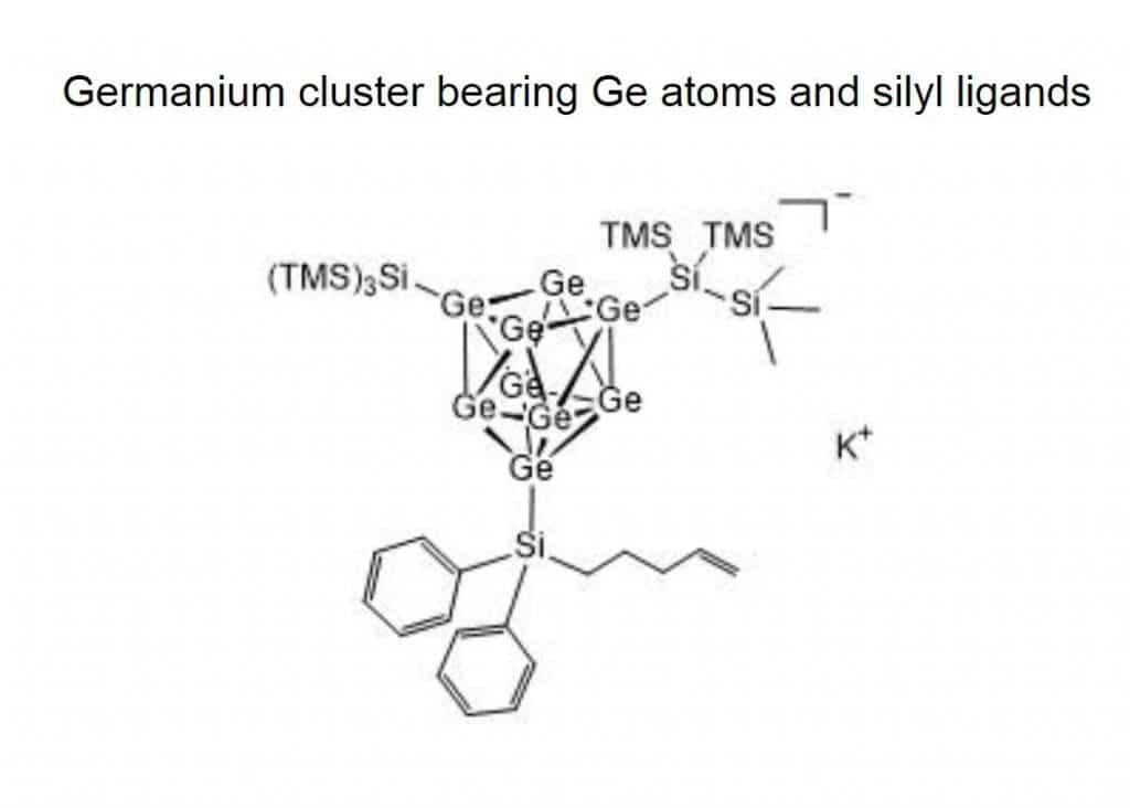
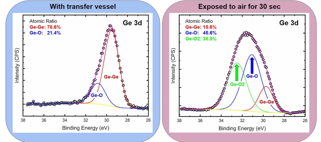
Comparison of XPS results of a Germanium cluster material that consists of Ge atoms and silyl ligands between (1) using the transfer vessel and (2) short exposure to air, demonstrates the samples are well preserved by the transfer vessel to avoid oxidation. Sample courtesy: Christoph Wallach, Jonathan Veinot, Department of Chemistry, University of Alberta
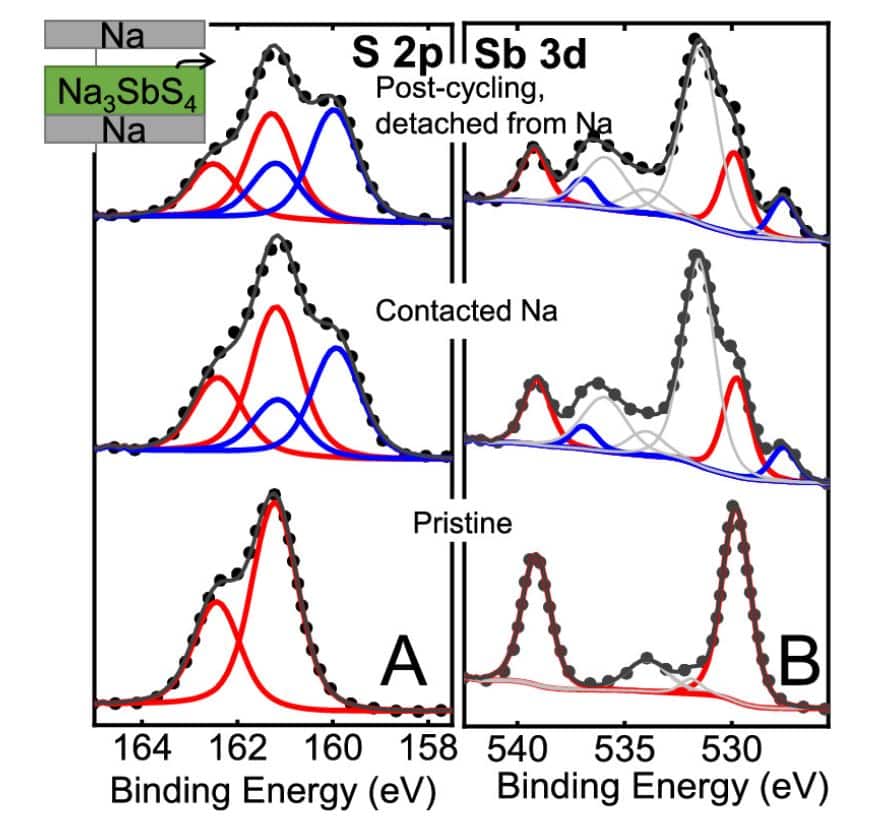
Prof. Lingzi Sang group at the Department of Chemistry, University of Alberta, has successfully characterized Na3SbS4/Anode Interface in All-Solid-State Sodium Battery, by utilizing the setup. For more details, please check their recent publication in ACS Appl. Mater. Interfaces 2022, 14, 48705−48714.
The process is now open to general users. If you are interested in XPS analysis of air-sensitive materials, please submit a sample analysis request on LMACS. If you have any questions, please feel free to contact Peng Li (Peng.Li@ualberta.ca) – the Characterization Group Manager.
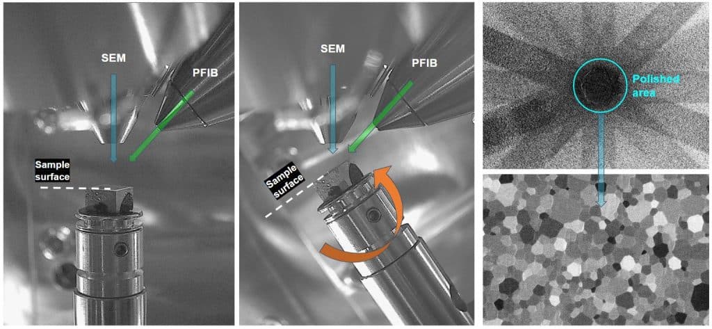
Spin Mill with Plasma FIB
A new approach – Spin Mill, for large-area planar milling with ion beams is now available on the Thermo Fisher Helios Hydra Plasma FIB/SEM for accessing and investigating large areas (up to 1 mm).
The Spin Mill method offers alternative planar sample preparation, expanding the PFIB-SEM application beyond the conventional cross-section technique and Broad Ion Beam (BIB) milling. In combination with the flexibility of multi-ion milling, Spin Mill provides site-specific large area processes for various types of materials, which enables new characterization capabilities previously considered challenging.
Spin Mill setup in Hydra PFIB
In the Spin Mill setup, the sample is mounted horizontally on the stage. The stage is tilted negatively, so that the PFIB beam mills the sample surface at a nearly glancing angle (typically between 1 and 5 degrees). The stage is periodically rotated through a full rotation of 360 degrees, which results in uniform planar polishing.
EBSD applications
While the Spin Mill application offers new capabilities in a wide range of materials characterization, several groups have benefited from it for their EBSD analysis.
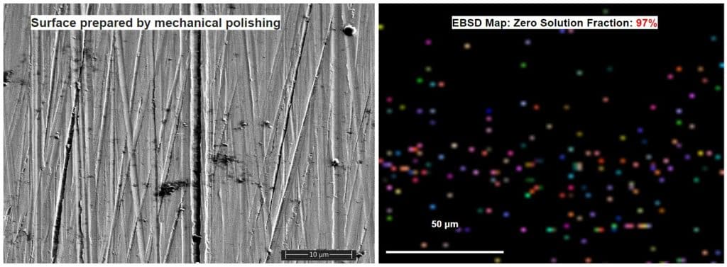
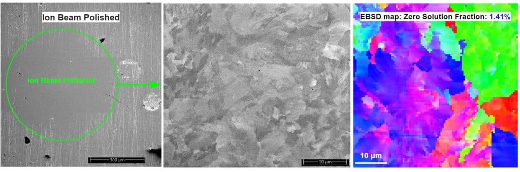
Sample: Rail Steel
Sample Courtesy: Stephen Okocha, Drs. Ben Jar and Michael Hendry, Mechanical Engineering Department, Civil and Environmental Engineering Department, Faculty of Engineering, University of Alberta
Xe ion beam was used as a general polishing of a rough surface after mechanical polishing. Hit rate was increased from 3% to 98.6% after ion beam polishing.
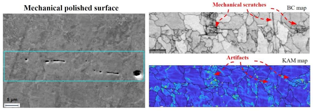
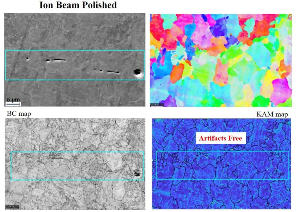
Sample: Steam pipe welds in power and heat supply line for mining of natural resources
Sample Courtesy: Yajing Wang, Dr. Leijun Li, Chemical and Materials Engineering Department, Faculty of Engineering, University of Alberta
Shallow mechanical scratches and small porosity effects on EBSD are removed by Xe ion beam polishing.
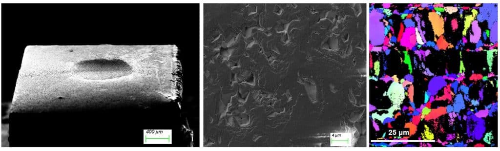
Sample: 3D printed Alumina for structural applications, including protection, aerospace coating&components and filtration systems.
Sample Courtesy: Cass (Haoyang) Li, Dr. James Hogan, Mechanical Engineering Department, Faculty of Engineering, University of Alberta
The Spin Mill method effectively polishes porous structures due to glancing incident angle to produce smooth surface for meaningful EBSD analysis.
If you need to process your samples by ion beam spin mill, please submit a “sample” request with sample details on LMACS. If you have any questions, please feel free to contact Peng Li (Peng.Li@ualberta.ca) – the Characterization Group Manager.
nGauge AFM is now Available at nanoFAB
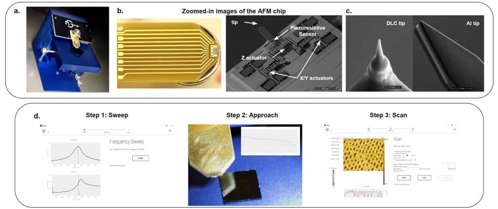
The nanoFAB is pleased to announce that the new Atomic Force Microscopy system, the ICSPI nGauge AFM, has been successfully installed and is operational now. This benchtop AFM allows nanoscale topography data collection with 3 easy steps: automatic sweep, approach, and scan. The nGauge AFM is a laserless system, based on a patented AFM-on-a-chip technology. In this new technology, all of the sensors and scanners of a traditional AFM have been integrated onto a single chip, so you can capture routine scans in just over a minute.
The nGauge AFM operates in the tapping mode and generates topography, phase, and error images simultaneously for any solid samples (including conductive and non-conductive, but not liquid samples). nGauge AFM tips are made of durable materials like diamond-like carbon (DLC) and aluminum oxide, which are also integrated onto the AFM chip, enabling hundreds (or thousands) of scans possible with each tip.
(a) The benchtop nGauge AFM. (b) AFM chip and its integrated components. (c) Front view of the Diamond-Like Carbon and Aluminum tips. (d) 3-step scan collection via nGauge AFM
nGauge AFM Specifications:
Max scan area: 20 x 20 μm
Z Range: 10 μm
Scan speed: 80 seconds (256 x 256 pixel, 20 x 20 μm)
Max scan resolution: 1024 x 1024 pixels (5 minutes)
Noise floor: <0.5 nm rms
XY Scanner resolution: <0.5 nm
Images: Topography, Phase, Error
Approach: Automatic
Max sample size: 100 mm x 50 mm x 16 mm
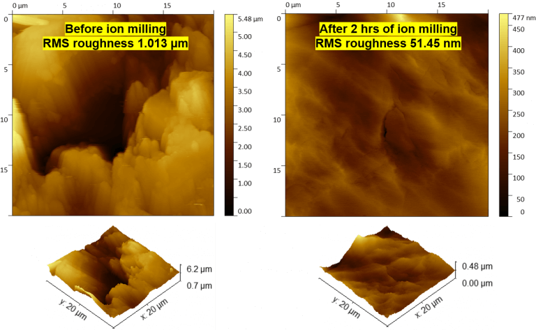
Sample: Shale (before and after ion milling processes) Sample courtesy of Graham Spray, M.Sc., P.Geo., AGAT Laboratorie.
Diamond-Like Carbon (DLC) Tip Specification:
nGauge AFM tips are made of diamond-like carbon materials with high aspect ratio offering excellent lateral resolution and excellent contamination resistance.
Tip radius: <20 nm
Tip height: >1 μm
Cone angle: <10°
Aspect ratio: >3
Tilt compensation: 15°
Tip post height: 3 μm
Tip shape: Conical
Tip material: Diamond-like carbon\
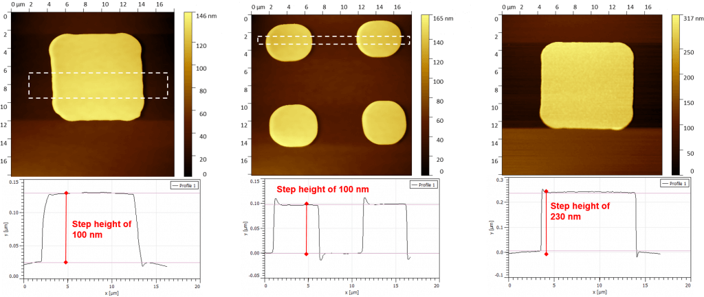
Sample: Patterned Cr + Au / Ti on Si chip
Cantilever Specifications:
nGauge AFM tips are located at the very end of the cantilever beam and are integrated onto a micro-electro-mechanical systems (MEMS) chip. The chip features integrated lateral and vertical actuators and piezoresistive sensors.
Shape: Beam
Length: 30 μm
Width: 6 μm
Thickness: 3 μm
Resonant Frequency: 8 kHz (typical: 7.3–8.7 kHz)
Stiffness: 0.1 N/m
The nGauge AFM is now available to users for both staff analysis and self-use/user training provided they purchase own nGauge AFM chip. Any users interested in getting trained on this tool or staff analysis should submit a request via LMACS. If you have any questions, please contact Dr. Nas Yousefi or Peng Li – the Characterization Group Manager.
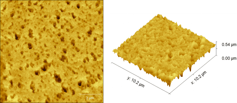
Sample: Polymeric Membrane Sample courtesy of Dr. Sadrzadeh, Mechanical Engineering Department, Faculty of Engineering, University of Alberta.