Raith_GDSII toolbox documentation now on Read The Docs
Now in its tenth year of existence, the Raith_GDSII MATLAB toolbox makes it easy to generate patterns for Raith electron-beam lithography (EBL) and focused ion beam (FIB) applications using MATLAB. It can also be used to generate “plain” (non-Raith-dialect) GDSII files for non-EBL applications such as printing photomasks or direct-write laser lithography exposures. This open-source project is maintained by the nanoFAB, may be downloaded from GitHub.
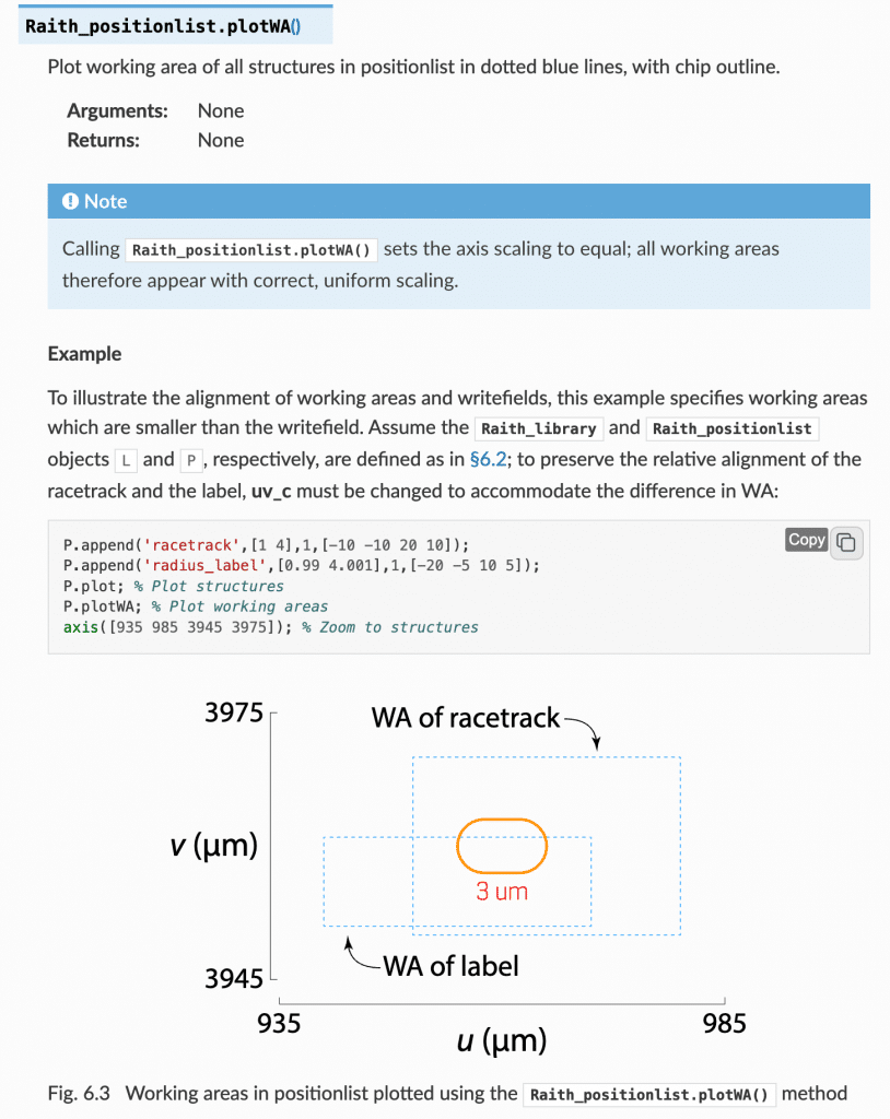
As of the most recent update, the technical documentation for the toolbox is now hosted online on Read the Docs, as opposed to the PDF user manual which served as documentation for previous versions.
This switch to online documentation ensures the documentation is always up to date (rebuilt with each GitHub commit), and includes quality of life improvements such as copy-to-clipboard buttons on all code block examples and a “search as you type” feature. This update also includes a small bugfix relating to outputting FBMS path elements with curvature in “plain” GDSII dialect, as well as several typographical edits to the documentation content.
We are excited about the potential of this updated documentation format to simplify and enhance both the initial learning and ongoing utilisation of the Raith_GDSII toolbox, for anyone interested in EBL, FIB, or other lithographic techniques. For more information, please contact Aaron Hryciw.
- Download – GitHub: github.com/ahryciw/Raith_GDSII
- Documentation – Read the Docs: raith-gdsii.readthedocs.io