Electron & Ion Microscopy (SEM, FIB and TEM) provides morphological and compositional analysis with ultra high spatial resolution but lack of larger macroscopic context. It is also challenging to obtain analysis and observations with multiple sources from identical locations of the same devices/samples, in order to obtain comprehensive data.
Software solutions are now installed and commissioned in the following microscopes, providing large area imaging and correlative workflow:
ATLAS on Zeiss Sigma FESEM ATLAS on Zeiss EVO SEM MAPS on ThermoFisher Hydra Plasma FIB/SEM
These software packages enable automatic workflow of multi-scale (from cm to nm), multi-platform (optical, x-ray, electron and ion microscopy and spectroscopy) and multi-dimensional (2D, 3D and 4D) characterization. Please see the application examples below of how the workflow can provide correlative analysis by linking Optical, Raman, AFM, XRM, SEM, FIB, and TEM data.
ATLAS and MAPS software are now available for user training. If you are interested in utilizing the workflow for your material characterization, please submit a training request on LMACS. If you have any questions, please feel free to contact Shihong Xu (shihongx@ualberta.ca), Josh Perkin (jperkins@ualberta.ca) or Peng Li (peng.li@ualberta.ca).
Application Examples
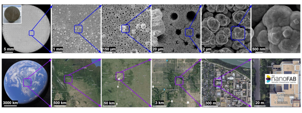
Sample: Porous Ni film Application: Large area imaging for multi-scale analysis (Google Earth like images with high spatial resolution) Instrument: Zeiss Sigma FESEM
A series of images seamlessly integrates correlative imaging to showcase a progressively zoomed view from a large object to a microscopic structure, transitioning from a satellite view of Earth to the intricate details of building layouts.
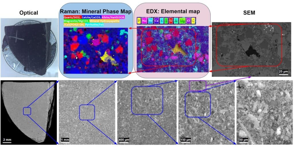
Sample: Shale Application: Multi-scale and correlative SEM/EDX/Raman analysis of elemental and mineral distribution Instruments: Zeiss EVO SEM with Oxford EDX Renishaw inVia Confocal Raman
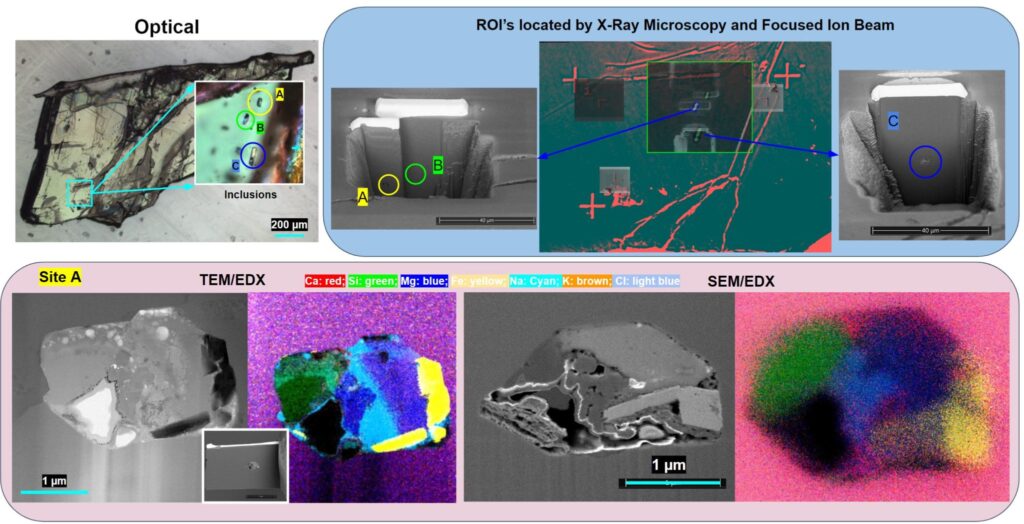
Sample: Mineral inclusions Application: Multi-scale and correlative SEM/EDX/XRM/TEM analysis of mineral inclusions in magnetite-apatite deposits This work is published in Geology (2024) 52 (6): 417–422
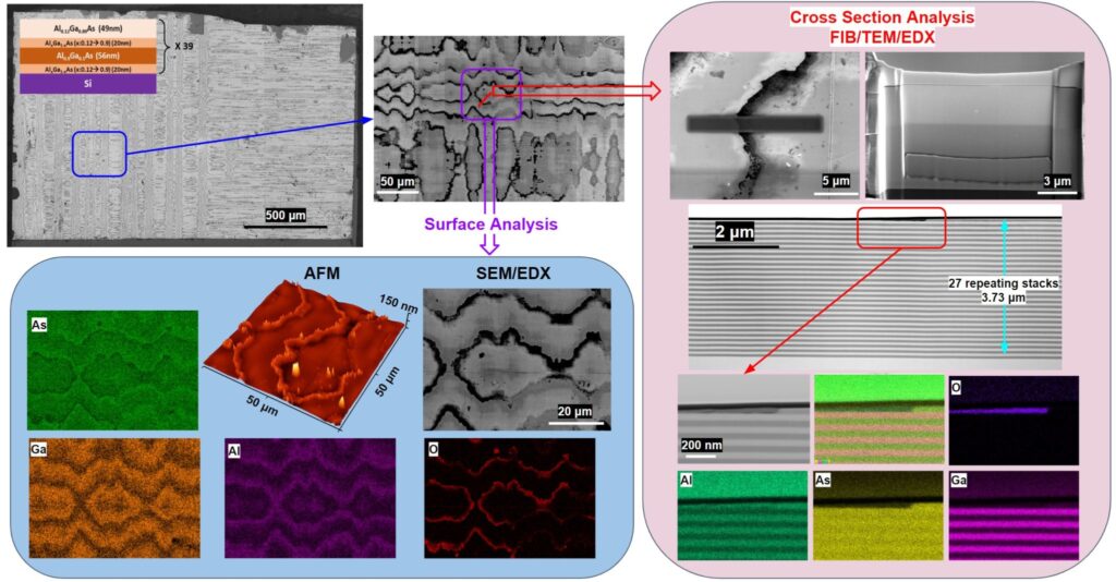
Sample: Multi-layer AlGaAs thin film Application: Correlative SEM/EDX/AFM/TEM analysis to characterize both surface and cross section morphology and composition Instruments: ThermoFisher Hydra Plasma FIB/SEM Bruker Dimension Edge AFM JEOL ARM S/TEM
Advanced TEM Sample Preparation
Focused Ion Beam (FIB) provides preparation of site-specific, high-quality S/TEM samples for a wide range of materials. Unlike the conventional Ga-FIB, which has slow milling rate, results in Ga damage/implantation, the ThermoFisher Helios Hydra Plasma FIB (equipped with multiple inert ion species - Xe and Ar) overcomes those unwanted effects and produces damage free TEM lamellas./
The latest technological innovations on the Hydra PFIB microscope, such as flexible control of micro-manipulator and stage, multi-precursor gas injection system (GIS), along with well integrated software solutions, enable fast and easy lamella preparation with high throughput for TEM analysis, less dependent on the operators’ experience.
Our Characterization team is pleased to announce that all advanced processing for TEM lamella preparation on the Hydra PFIB have been successfully commissioned, including:
Low voltage Xe and Ar beams to produce damage free samples
Micro-manipulator (EasyLift) with continuous axial rotation, enabling flexible pluckouts, such as 90-degree / inverted pluckouts for both cross-sectional and plan-view preparation.
Multiple precursors for Gas Injection System (GIS): C, Pt, W, providing flexible capping films for materials with different hardness and backfilling for porous materials.
Automatic Lamella Sample preparation: fully automatic site preparation and software-assisted pluckout and final polishing.
Our user groups have utilized those techniques to produce TEM samples for their characterization needs. If you are interested in preparing TEM lamellas on the Hydra PFIB system, user training and staff analysis are available. Please submit a request (training or sample type) with sample details on LMACS. If you have any questions, please feel free to contact Dr. Shihong Xu (shihongx@ualberta.ca) - PFIB, Xuehai Tan (xtan@ualberta.ca) - TEM or Peng Li (peng.li@ualberta.ca) – the Characterization Group Manager.
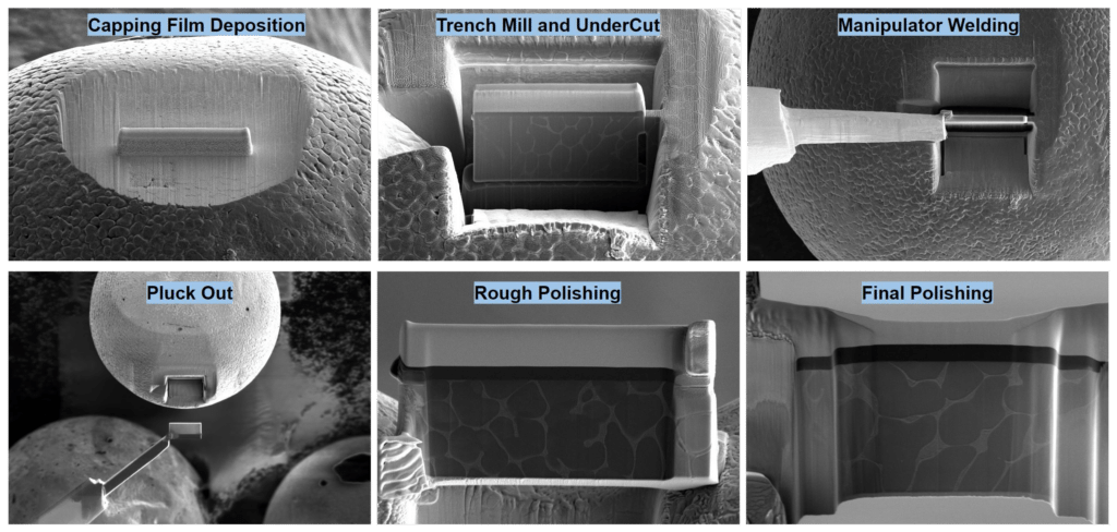
Standard Lamella Preparation
Series of six images illustrating stages in advanced TEM sample preparation: capping film deposition, trench milling and undercutting, manipulator welding, plucking out, rough polishing, and final polishing.
Application Examples
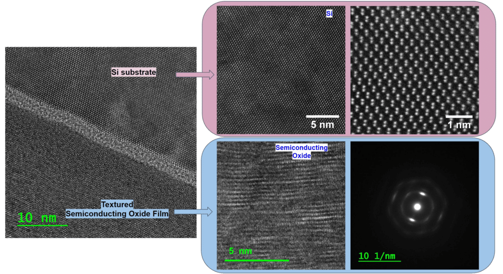
Sample: Semiconducting Oxide Film on Si FIB Application: Low voltage 2kV Ar polishing to produce damage free sample for HR-STEM imaging Sample Courtesy: Avalon Holographics Inc., Edmonton
Microscopic images reveal the Si substrate (upper panel) and a textured semiconducting oxide film (lower panel), featuring distinct nano-scale structures and electron diffraction patterns, achieved through advanced TEM sample preparation techniques.
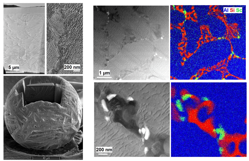
Sample: Rapidly solidified Al-10Si-0.4Sc droplets (atomized using Impulse Atomization) FIB Application: Flexible micromanipulation to pluckout samples from spheres Sample Courtesy: Akki Sahoo, Dr. Jonas Valloton and Prof. Hani Henein, Faculty of Engineering, University of Alberta; Abdoul-Aziz Bogno, Equispheres Inc., Ottawa
A collage of microscopic images, prepared with advanced TEM techniques, showcases various materials' textures and compositions with scale bars. The top right image features a color map, highlighting elements labeled as Al, Si, and Sc.
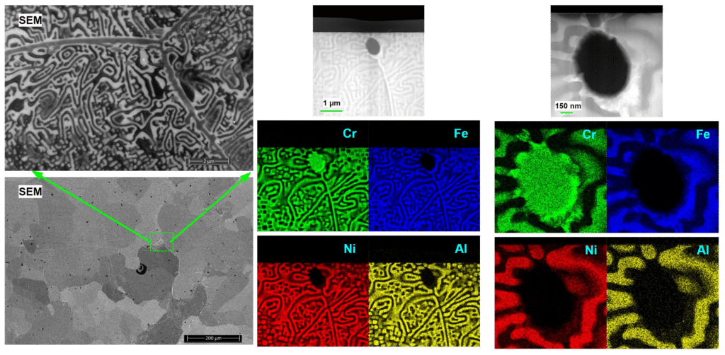
Sample: Al-Cr-Fe-Ni medium-entropy alloy (MEA) FIB Application: Mixed Pt/C capping film for effective protection for HEA/MEA materials Sample Courtesy: Guijiang Diao and Prof. Dongyang Li, Faculty of Engineering, University of Alberta
A series of SEM and color maps displaying material composition, with elements Cr (green), Fe (blue), Ni (red), Al (yellow) on a patterned surface. Focus is on a circular area, highlighting the precision in sample preparation for Advanced TEM analysis.
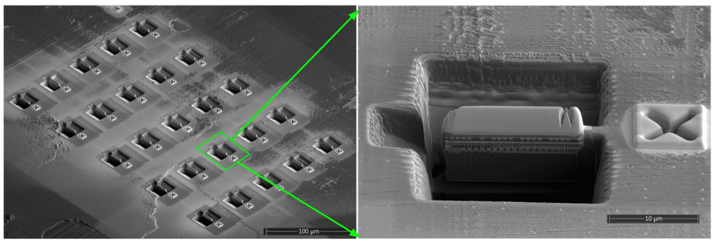
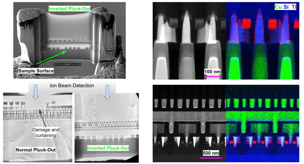
Sample: Intel Core i7 processor FIB Application: Inverted pluckout to reduce curtaining and damage in the regions of interest.
Advanced TEM images reveal semiconductor structures with ion beam detection, highlighting inverted pluck-out areas. Color coding indicates elements: Cu, Si, Ti, ensuring precise TEM sample preparation for detailed analysis.
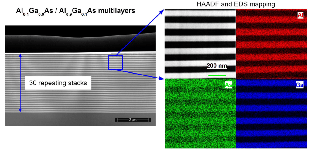
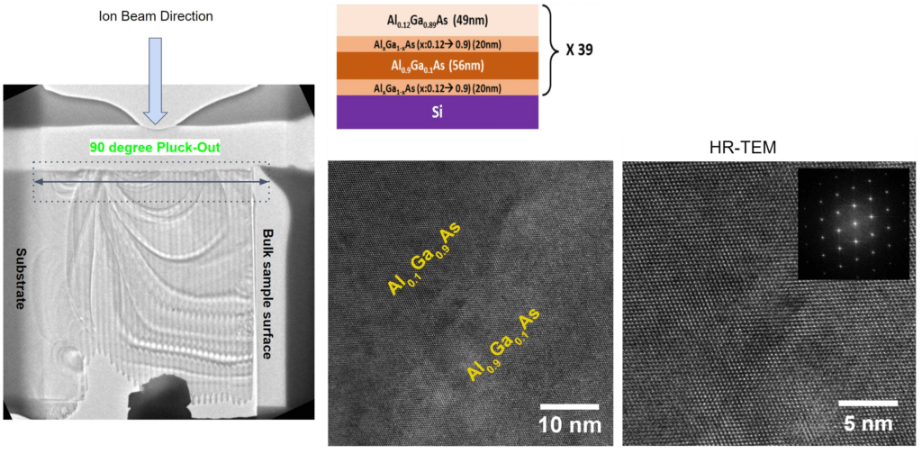
Sample: AlGaAs multilayers FIB Application: 90-degree pluckout (ion beam parallel to the layer stacks) to produce uniform thin thickness across all layers.
A semiconductor cross-section reveals layers of Al₀.₃Ga₀.₇As and Al₀.₄₅Ga₀.₅₅As on Si, with advanced TEM images and a diffraction pattern presented on the right, highlighting meticulous sample preparation techniques.Advanced TEM nanobeam diffraction images reveal crystallographic mismatch in Al[_x]Ga[_{1-x}]As/Al[_y]Ga[_{1-y}]As layers, complemented by a selected area electron diffraction pattern.Microscopic image of AlGaAs/AlGaAs multilayers displaying 30 repeating stacks. Includes HAADF and EDS mapping with highlighted elements: Al in red, As in green, Ga in blue. Advanced TEM sample preparation showcases intricate layer details for accurate analysis.
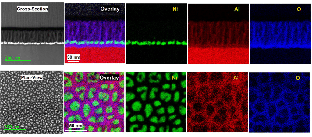
Sample: Nano-composite material (Ni nanoparticles in anodized Al) FIB Application: Flexible miro-manipulation to produce cross-sectional and plan-view lamellas Sample Courtesy: Dr. Matthew Nickel and Prof. Todd McMullen, Faculty of Medicine & Dentistry, University of Alberta
Advanced TEM cross-sectional and plan-view microscopy images reveal distributions of Ni, Al, and O with remarkable clarity. The cross-section shows stratified layers, while the plan-view features patchy clusters. Scale bars are set at 200 nm and 50 nm respectively.
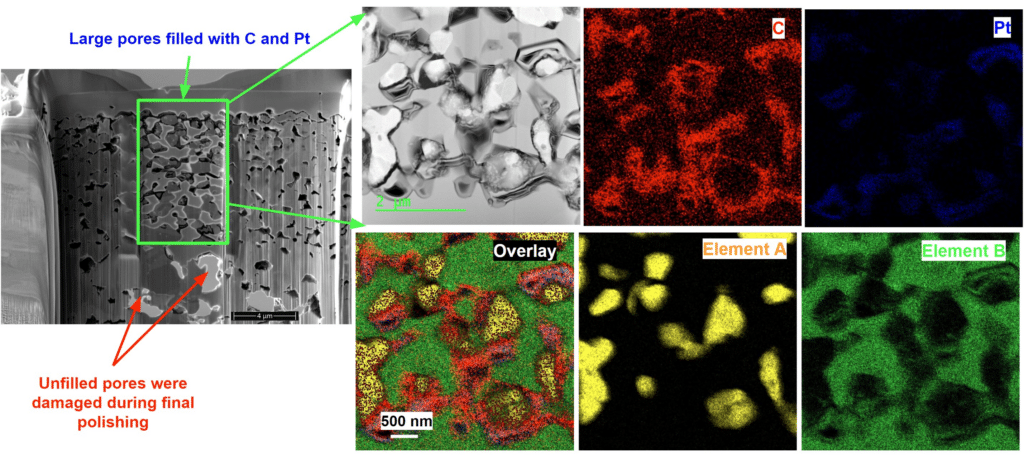
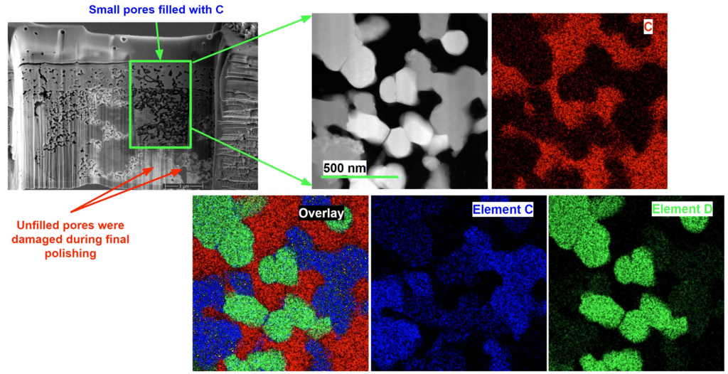
Sample: Porous solid oxide fuel cell FIB Application: Back-filling with in-situ GIS to prepare high quality samples from porous materials. Sample Courtesy: Prof. Douglas Ivey, Faculty of Engineering, University of Alberta
Microscopic images using advanced TEM reveal pores, element concentration maps, and overlays; highlighting small carbon-filled pores and unfilled, damaged pores.
Sample: Intel Core i7 processor FIB Application: Fully automatic/unattended site preparation of 25 locations
A grayscale image showcasing a zoomed-in view of microstructures highlights an inset detailing a close-up of one microstructure, prepared using Advanced TEM techniques, featuring a rectangular shape inside a square cavity.
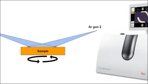
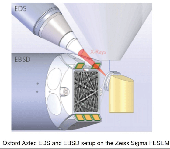
Broad Ion Beam (BIB) polishing for SEM/EDX/EBSD
The RES 102 system features:
Ion energy: 0.8 to 10 keV
Source current: Up to 4.5 mA
Stage Rotation: 0.6 to 10 rpm
Sample size SEM holder: max. Ø 25 mm × 12 mm
Prepared area SEM holder: max. Ø 25 mm
RES102 BIB Ion Milling System equipped with two Ar guns
Among general electron microscopy applications, Electron Backscatter Diffraction (EBSD) is a surface technique – typical probing depth is in the range of a few tens nm for a beam energy of 20 kV. Smooth and damage-free surface is critically important to obtain high quality EBSD data. Compared to conventional mechanical polishing techniques, which can result in very rough surfaces and a thick damaged layer, low energy beam at grazing incident angle and rotating stage on the RES102 can effectively polish the surface to reduce roughness and remove the damaged layer.
With the programmable recipes of flexible parameters (beam energy, beam current, incident angle, stage rotating speed), the RES102 BIB has produced very nice results for our users for EBSD analysis. See recent examples below.
Application Examples (EBSD)
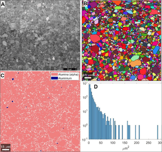
Sample: 3D printed Alumina for structural applications
Sample Courtesy: Cass (Haoyang) Li, Dr. James Hogan, Mechanical Engineering Department, Faculty of Engineering, University of Alberta
Ion Milling process:
8 kV, 3 mA, 3.5 degrees, 1.5 rmp for 120 mins
8 kV, 2 mA, 2.5 degrees, 1.5 rmp for 60 mins
EBSD mapping: 175 µm x 175 µm, stepsize 50 nm
(A) SEM image; (B) Orientation map; (C) Phase maps of Alumina and Aluminium; (D) Grain size distribution
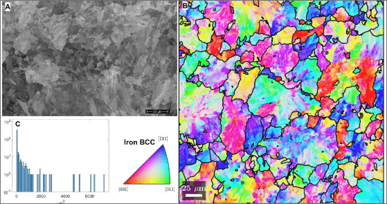
Sample: Rail Steel
Sample Courtesy: Stephen Okocha, Drs. Ben Jar and Michael Hendry, Mechanical Engineering Department, Civil and Environmental Engineering Department, Faculty of Engineering, University of Alberta
Ion Milling process:
8 kV, 3 mA, 2.5 degrees, 1.5 rmp for 60 mins
6 kV, 2 mA, 2.5 degrees, 1.5 rmp for 60 mins
EBSD mapping: 300 µm x 300 µm, stepsize 250 nm
(A) SEM image; (B) Orientation map; (C) Grain size distribution
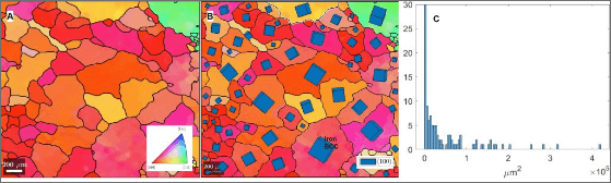
Sample: Al-Cr-Fe-Ni medium-entropy alloy (MEA)
Sample Courtesy: Guijiang Diao, Dr. Dongyang Li, Chemical and Materials Engineering Department, Faculty of Engineering, University of Alberta
Ion Milling process:
8 kV, 3 mA, 3.5 degrees, 1.5 rmp for 60 mins
5 kV, 2 mA, 2.5 degrees, 1.5 rmp for 60 mins
EBSD mapping: 2500 µm x 1500 µm, stepsize 500 nm
(A) Orientation map; (B) Crystal unit cell orientation and (C) Grain Size Distribution
The RES102 ion milling system is now available to general users for both staff analysis and user training. Any users interested in getting trained on this tool or staff analysis should submit a request on LMACS. If you have any questions, please contact the tool managers Drs. Nas Yousefi and Shihong Xu or Peng Li – the Characterization Group Manager
FIB/SEM tomography is a high-resolution 3D volume analysis technique, by serial sectioning – sequential application of SEM imaging and FIB milling.
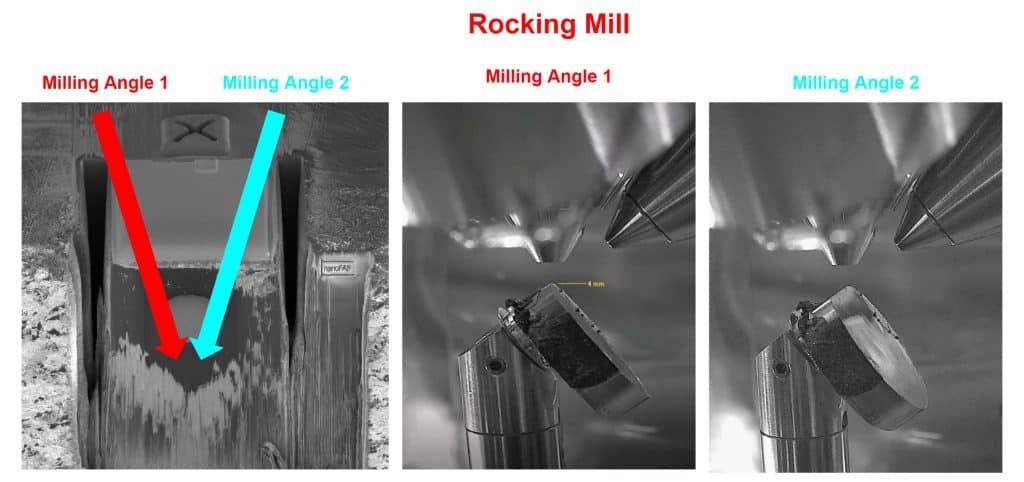
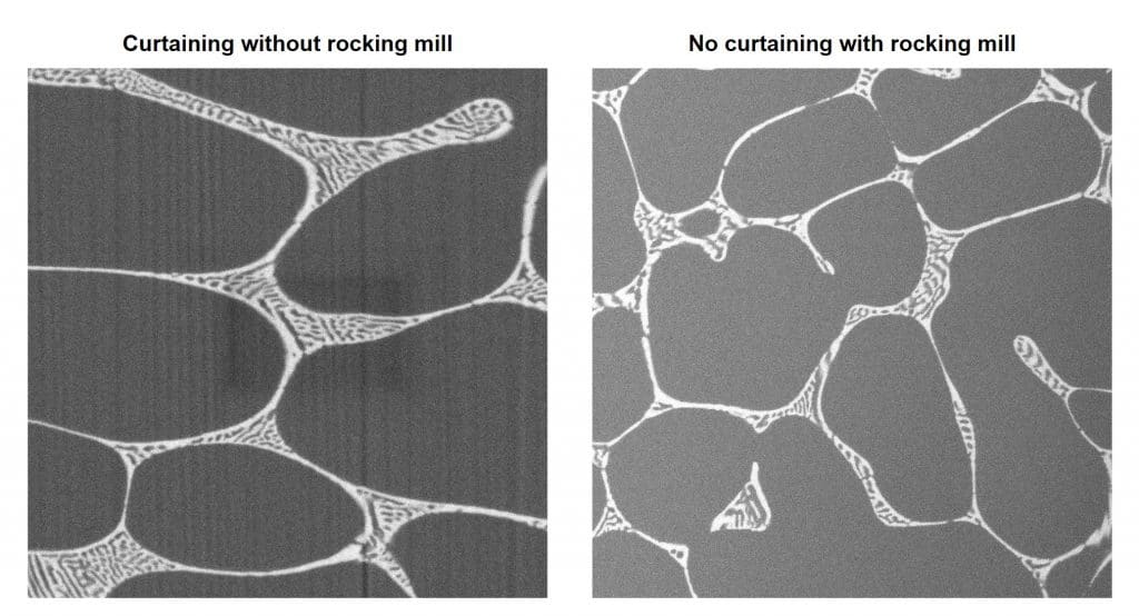
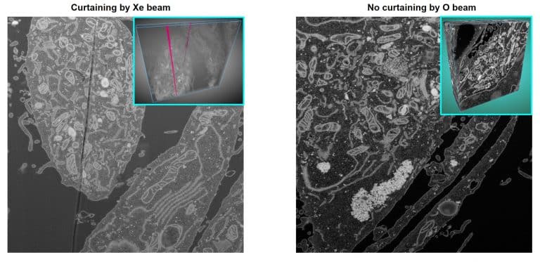
Rocking mill minimizes curtaining effect
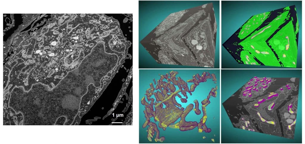
3D reconstruction of Mitochondria in Hela cells Sample Courtesy: Drs. Thomas Simmen, Mike Hendzel and Xuejun Sun, Faculty of Medicine and Dentistry, University of Alberta Process details: Volume 1: O beam, 30 kV, 1.7 nA, 3 nm slice thickness, 4550 slices Volume 2: Xe beam, 30 kV, 4 nA, 5 nm slice thickness, 5990 slices
Multiple ion species (Xe, Ar, O, or N) are available, enabling optimal ion beams for various types of materials. While Xe beam is suitable for general inorganic materials, Oxygen ions provide much better milling quality for biological samples embedded in resins, in terms of less milling artifacts.
The ASV FIB/SEM tomography process is now available to users as staff analysis. If you have needs for these analysis, please submit a “sample” request with sample details on LMACS. If you have any questions, please feel free to contact Peng Li (Peng.Li@ualberta.ca) – the Characterization Group Manager.
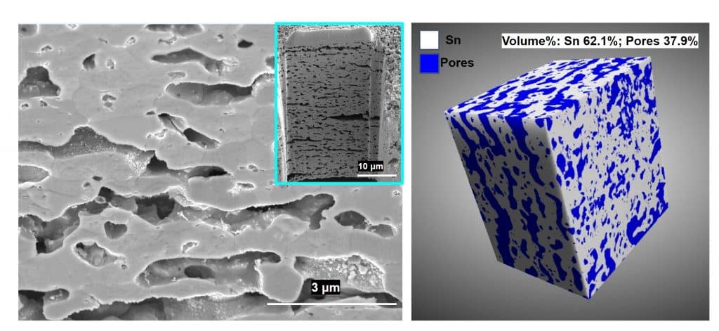
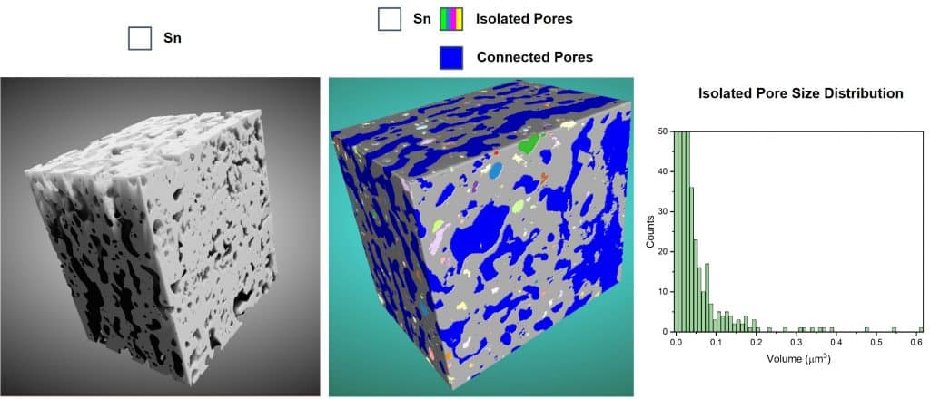
Porosity analysis of Porous Sn Sample Courtesy: Drs. Peter Kalisvaart, Jillian Buriak (University of Alberta) and Bing Cao (Nanode Battery Technologies) Process details: Xe beam, 30 kV, 4nA, 10 nm slice thickness, 895 slices
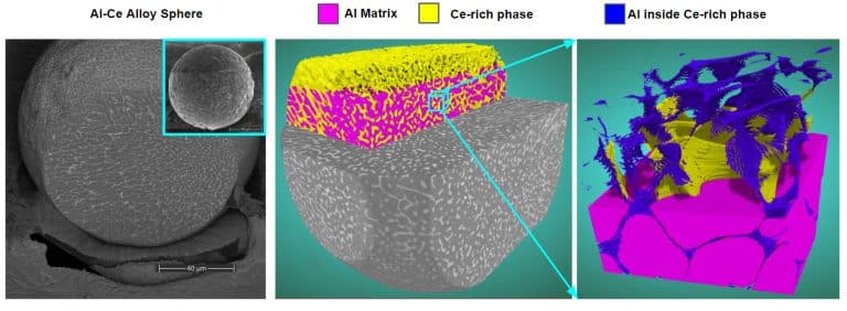
3D reconstruction of Al and Ce phases in Al-Ce alloy spheres Sample Courtesy: Drs. Jonas Valloton and Hani Henein, Faculty of Engineering, University of Alberta Process details: Volume 1: Low Mag./large volume, Xe beam, 30 kV, 4 nA, 30 nm slice thickness, 2179 slices Volume 2: High Mag./small volume, Xe beam, 30 kV, 4 nA, 5nm slice thickness, 1220 slices
New nanoFAB Characterization Staff
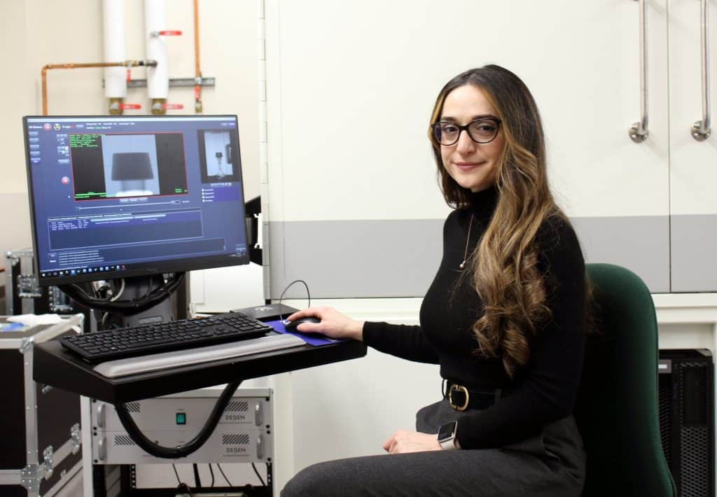
The nanoFAB is pleased to announce a new Applications/Research Specialist staff member – Dr. Nastaran (Nas) Yousefi in our Characterization group.
Nas is a physical/materials chemist with extensive research background in organic optoelectronic materials. During her PhD, she gained considerable experience with fabrication processes for organic electronics (e.g., transistors, biosensors), materials characterization (e.g., AFM, HIM, GIXAS), and electrical characterization techniques. Given the multidisciplinary nature of her research projects in the past, she has acquired a unique skillset that complements the expertise and capabilities at nanoFab.
Nas’ primary areas of responsibility are XRM, XRD/SAXS, BET, spectroscopy and electrical characterization/test tools. She will be working to support user training, fee-for-service work and process development. She is beyond excited to help researchers navigate through their path of discoveries and train students to become independent researchers.
Please join us in welcoming Nas!
Dr. Nas Yousefi in the Zeiss Xradia Versa 620 X-Ray Microscopy Lab
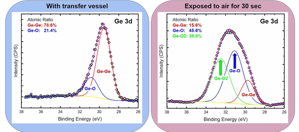
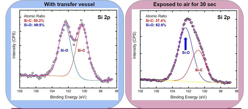
XPS analysis of air-sensitive materials
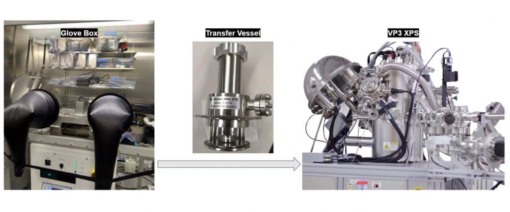
The nanoFAB is pleased to announce that analysis of air-sensitive materials is available on the PHI VP3 XPS system.
Proper sample handling is critical to analyze materials that are sensitive to air. We have been working to bring the capabilities of analyzing air-sensitive materials on to our analytical instruments. A controlled-environment transfer vessel is now commissioned and available to transfer samples from glove boxes to the PHI VP3 Versa Probe III XPS to minimize environmental exposure during sample transfer/loading.
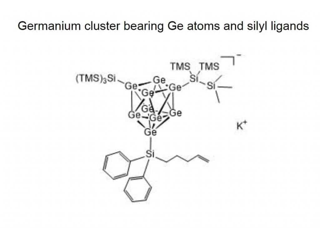
Comparison of XPS results of a Germanium cluster material that consists of Ge atoms and silyl ligands between (1) using the transfer vessel and (2) short exposure to air, demonstrates the samples are well preserved by the transfer vessel to avoid oxidation. Sample courtesy: Christoph Wallach, Jonathan Veinot, Department of Chemistry, University of Alberta
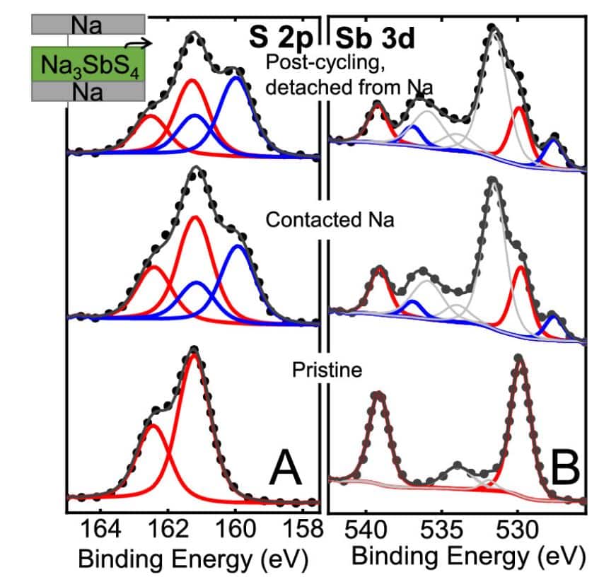
Prof. Lingzi Sang group at the Department of Chemistry, University of Alberta, has successfully characterized Na3SbS4/Anode Interface in All-Solid-State Sodium Battery, by utilizing the setup. For more details, please check their recent publication in ACS Appl. Mater. Interfaces 2022, 14, 48705−48714.
The process is now open to general users. If you are interested in XPS analysis of air-sensitive materials, please submit a sample analysis request on LMACS. If you have any questions, please feel free to contact Peng Li (Peng.Li@ualberta.ca) – the Characterization Group Manager.
![Advanced TEM nanobeam diffraction images reveal crystallographic mismatch in Al[_x]Ga[_{1-x}]As/Al[_y]Ga[_{1-y}]As layers, complemented by a selected area electron diffraction pattern.](https://www.nanofab.ualberta.ca/wp-content/uploads/2025/02/06b-Al-Ga-As-1024x410.png)