Optical Emission Interferometry (OEI) in the Plasma-Therm Versaline PECVD

Overview

In plasma-enhanced chemical vapour deposition (PECVD) tools, the deposition rate of deposited films can often fluctuate with relative gas concentrations, material build-up on the chamber walls, and other mechanisms that make timed depositions inconsistent. To combat this problem, a simple technique called Optical Emission Interferometry (OEI) can be used. OEI provides a more robust form of deposition control based on the interference of light reflected off of the growing film to precisely hit target film thicknesses.

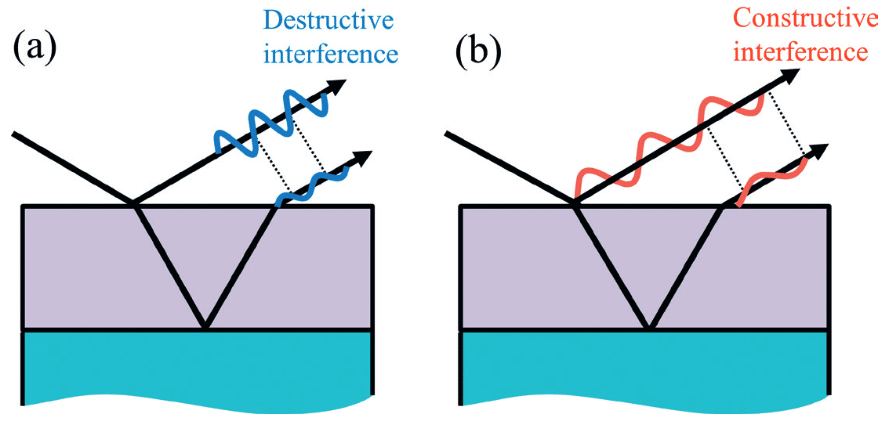
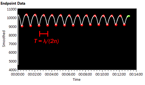
OEI uses similar principles to other interferometric tools like the Filmetrics F50-UV; the intensity of light at a single wavelength reflected off of a thin film will vary depending on the wavelength of light and the optical thickness of the film. This is due to the relative phase difference between light reflected off the top surface of the film and at the film-substrate interface, i.e., conditions of constructive and destructive interference (shown in Fig. 1). Across a broad spectrum of wavelengths, this can be used to fit to both refractive index and film thickness robustly (as Filmetrics does). However, if the intensity of light reflected off of a growing film is recorded continuously, the intensity at a "single" wavelength will oscillate approximately sinusoidally as the thickness increases (satisfying constructive and destructive interference conditions at specific thicknesses)—this is the fundamental premise of OEI. By noting when the extrema occur during film growth, the period of this oscillation (T) can be used to measure the deposition rate of the film, since T is set by the phase conditions for constructive/destructive interference. T = λ/(2n); where λ is the wavelength of interest and n is the refractive index of the material at this wavelength.

Diagram illustrating (a) destructive and (b) constructive interference, incorporating the principles of Optical Emission Interferometry. Two waves reflect off surfaces, with destructive showing out-of-phase and constructive in-phase interactions.
Figure 1. Phase conditions for destructive and constructive interference of light reflected off of a thin film, from H. G. Tompkins, and J. N. Hilfiker, Spectroscopic Ellipsometry: Practical Application to Thin Film Characterization (Momentum Press, 2016).

To use OEI in the Plasma-Therm Versaline PECVD, light produced by the plasma is reflected off of the growing film and collected by a spectrometer centred above the wafer for plasma monitoring. The Plasma-Therm EndpointWorks software package is then used to monitor the evolution in time of the spectral intensity emitted from the plasma within a narrow range of wavelengths. Choosing a range that encompasses an emission line of a typical gas/radical species within the plasma produces the oscillatory data shown in Fig. 2. Values of T are calculated based on known values of n and λ to give an estimate of the deposition rate based on the spacing of the extrema. Thus, in order to function correctly, each OEI recipe requires the user to have knowledge of both the growing film (single wavelength refractive index) and of typical optical emission lines (usable wavelengths) within the plasma.

Graph titled "Endpoint Data" shows an oscillating white line with red and green highlights, likely depicting Optical Emission Interferometry data. The X-axis is time and the Y-axis is smoothed data. A red notation reads "T = λ/(2n)" with a horizontal bracket, possibly showcasing Plasma-Therm analysis.
Figure 2. EndpointWorks Thickness Detector data for a growing SiO2 film.

Wavelength choice

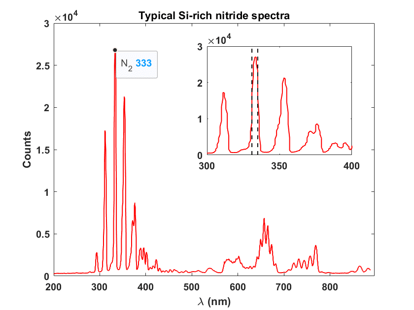
The choice of what wavelength to use for OEI depends on the chemistry of the plasma in question, since each gas/radical species emits light at different wavelengths (depending on its electronic transitions), and thus the available wavelengths will differ for each recipe. Potential emission lines are further limited if the gas species characteristic of an emission line is consumed during the reaction. The intensity of these reactant emission lines will fluctuate as the film grows and as the local gas concentration changes. In contrast, the intensity of an emission line of an inert gas (He, Ar, or N2 are often used to dilute the reactants) will be much more stable, and will provide a reduction in noise in the reflected light. This leads to a more clearly defined periodic signal, where the extrema can be easily identified in software. Additionally, since variation in T is linear with the wavelength of light used, the choice of shorter wavelengths will reduce the period of oscillation, lending the OEI method more sensitivity and flexibility to accurately measure thinner films. Note, for films that are optically absorbing (e.g. a-Si and Si-rich nitrides), the film will absorb more strongly at shorter wavelengths, decreasing the amplitude of the oscillation as the film grows. Ultimately, this decay reaches a point where extrema cannot be identified past a certain thickness. A general rule of thumb is to choose the shortest wavelength inert gas emission line that is not strongly absorbed by the depositing film. A typical spectrum collected during deposition is shown in Fig. 3, where a N2 emission line at ~333 nm is highlighted, being suitable for the gas chemistry involved. For more details on choosing an emission line appropriate for your deposition, please see the Plasma-Therm Versaline PECVD OEI recipe development How-To on the nanoFAB's Confluence Knowledge Base.

Graph showing Si-rich nitride spectra with wavelength (nm) on the x-axis and counts on the y-axis, using Plasma-Therm's Optical Emission Interferometry. Main peak at 333 nm. Inset shows detailed view of 300-400 nm range with multiple peaks.
Figure 3. Typical plasma emission spectrum (as measured on the Versaline's integrated Ocean Optics spectrometer) for the deposition of Si-rich nitride. Inset: full-width at half-max (dashed lines) of the N2 emission line centred at ~333 nm.

OEI controlled deposition recipes are currently qualified for SiO2 Dep ("OEI SiO2 Dep") and Stoichiometric Nitride ("OEI Stoichiometric Nitride") recipes, with an OEI recipe in progress for the Si-Rich Nitride. For user-developed films that differ from these established recipes, users are welcome to qualify their own OEI recipes following the Step-by-step instructions in the linked OEI recipe development How-To. If you encounter problems setting up your OEI recipe on EndpointWorks, please contact Tim Harrison (tr1@ualberta.ca).
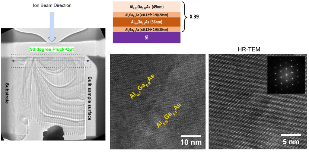
Correlative imaging workflow available on SEM/FIB

Electron & Ion Microscopy (SEM, FIB and TEM) provides morphological and compositional analysis with ultra high spatial resolution but lack of larger macroscopic context. It is also challenging to obtain analysis and observations with multiple sources from identical locations of the same devices/samples, in order to obtain comprehensive data.

Software solutions are now installed and commissioned in the following microscopes, providing large area imaging and correlative workflow:

ATLAS on Zeiss Sigma FESEM
ATLAS on Zeiss EVO SEM
MAPS on ThermoFisher Hydra Plasma FIB/SEM

These software packages enable automatic workflow of multi-scale (from cm to nm), multi-platform (optical, x-ray, electron and ion microscopy and spectroscopy) and multi-dimensional (2D, 3D and 4D) characterization. Please see the application examples below of how the workflow can provide correlative analysis by linking Optical, Raman, AFM, XRM, SEM, FIB, and TEM data.

ATLAS and MAPS software are now available for user training. If you are interested in utilizing the workflow for your material characterization, please submit a training request on LMACS. If you have any questions, please feel free to contact Shihong Xu (shihongx@ualberta.ca), Josh Perkin (jperkins@ualberta.ca) or Peng Li (peng.li@ualberta.ca).


Application Examples

Sample: Porous Ni film
Application: Large area imaging for multi-scale analysis (Google Earth like images with high spatial resolution)
Instrument: Zeiss Sigma FESEM

A series of images seamlessly integrates correlative imaging to showcase a progressively zoomed view from a large object to a microscopic structure, transitioning from a satellite view of Earth to the intricate details of building layouts.

Sample: Shale
Application: Multi-scale and correlative SEM/EDX/Raman analysis of elemental and mineral distribution
Instruments:
Zeiss EVO SEM with Oxford EDX
Renishaw inVia Confocal Raman


Sample: Mineral inclusions
Application: Multi-scale and correlative SEM/EDX/XRM/TEM analysis of mineral inclusions in magnetite-apatite deposits
This work is published in Geology (2024) 52 (6): 417–422

Instruments:
Zeiss Versa 620 X-Ray Microscope
ThermoFisher Hydra Plasma FIB/SEM
JEOL ARM S/TEM


Sample: Multi-layer AlGaAs thin film
Application: Correlative SEM/EDX/AFM/TEM analysis to characterize both surface and cross section morphology and composition
Instruments:
ThermoFisher Hydra Plasma FIB/SEM
Bruker Dimension Edge AFM
JEOL ARM S/TEM

AML Wafer Bonder now available for training

The nanoFAB is pleased to announce an upgrade to our wafer bonding and packaging area, with the recent installation of a wafer bonder from Applied Microengineering Ltd (AML).  The AWB-04 wafer aligner-bonder from AML offers a wide range of bonding techniques and process flexibility. Of particular note is its in situ alignment capability, allowing users to verify correct alignment as the wafers are being brought into contact.


Bonding techniques include:

Technical features:


Application Examples

Anodic Bond: borosilicate glass to Si

Cross-sectional SEM (left) and TEM (right) images of bonding interface.

Si–Si Direct Bond: in situ RAD + low-temperature anneal

TEM images of the bonding interfaces of silicon wafers after a low-temperature (250 °C) anneal performed in the AWB-04 chamber without breaking vacuum. The thin amorphous native SiO2 layer can be seen along the interface.

Si–Si Direct Bond: in situ RAD + external high-temperature anneal

TEM images of the bonding interfaces of silicon wafers after a high-temperature (1100 °C) anneal performed in Tystar General Anneal (Tube 6). The thin amorphous native SiO2 layer can be seen along the interface, but has diffused into the bulk Si layer.

Au–Au Thermocompression Bond: Si to Si with Au interlayers

SEM images of silicon wafers bonded via Au–Au thermocompression bonding: full wafer cross-section (left) and close-up of bond interface (right). Patterned Au films are deposited on Si wafers and bonded using moderate temperatures (~300 °C) and high pressures (~7.5 MPa). Images courtesy of Jones Microwave Inc. and RM3.

If you are interested in using the AML wafer bonder in your work, please submit a request through LMACS to receive training. If you have any questions, please feel free to contact Scott Munro or Aaron Hryciw.

New Spray Coating Tool Available

We are happy to announce a new addition to our fabrication tool lineup: a Sono-Tek ExactaCoat Spray Coater. This tool is located in our recently renovated 10k Lithography area (ECERF W1-031); please stay tuned over the coming months as we add more photolithography capabilities to this labspace.

The ExactaCoat, an ultrasonic spray coating system, can accommodate specimens up to 300 mm in diameter. This tool is primarily used for photoresist coating in situations where conventional spin coating is impractical or yields poor results: specimens that are too fragile, exhibit large topographical variations, or possess irregular shapes.

The spray coater offers a particular advantage for specimens where topography presents a challenge to achieving good film uniformity during spin coating: examples include MEMS or microfluidic devices with deep (tens to hundreds of µm) features etched via DRIE or KOH/TMAH. Process development is currently underway to formulate recipes suitable for coating deep and/or high aspect ratio topography wafers. Additionally, spray coating is a valuable technique for those looking to apply photoresist as a dicing protect layer on extremely fragile or through-etched substrates that are not compatible with spin coating.

Sono-Tek ExactaCoat Spray Coater
Illustration depicting stages of droplet formation: solvent evaporation in flight, landing on a substrate, and forming a closed resist film, annotated with arrows and text labels. The spray coating process is enhanced with our Spray Coating Tool available for precision applications.
Schematics of the spray coating process
(MicroChemicals)

The spray coating process uses high-frequency (ultrasonic) mechanical vibration that is transferred to the liquid in the nozzle. The standing waves created in the liquid are broken up as the liquid exits the nozzle—this aerosolised liquid is then dispensed onto the surface of the specimen as a fine mist.

 
To coat an extended specimen such as a wafer, the spray of atomised resist is rastered across the work area in overlapping stripes. This is illustrated in the following videos, where a cleanroom wipe is used to show the sprayed resist more clearly.

After spray coating a wafer with resist and softbaking, it may be exposed and developed to complete a photolithography process. The following optical microscope images illustrate some preliminary results of photolithography on Si wafers, showcasing excellent film uniformity and achieving lateral feature sizes as small as 5 µm.

Photolithography using spray coating: Si wafers spray coated with a ~4.5 µm thick film of AZ 1505, exposed in a contact mask aligner, and developed. The smallest feature size pictured in each image is 5 µm.

We are thrilled to introduce this new capability, along with the array of associated applications it makes possible. If spray coating is a technique you feel would be beneficial to your work, please submit a request through LMACS to receive training. If you have any questions, please do not hesitate to contact Breanna Cherkawski or Aaron Hryciw.

Resources

Application note: Spray coating (MicroChemicals GmbH)

Advanced TEM Sample Preparation

Focused Ion Beam (FIB) provides preparation of site-specific, high-quality S/TEM samples for a wide range of materials. Unlike the conventional Ga-FIB, which has slow milling rate, results in Ga damage/implantation, the ThermoFisher Helios Hydra Plasma FIB (equipped with multiple inert ion species - Xe and Ar) overcomes those unwanted effects and produces damage free TEM lamellas./

The latest technological innovations on the Hydra PFIB microscope, such as flexible control of micro-manipulator and stage, multi-precursor gas injection system (GIS), along with well integrated software solutions, enable fast and easy lamella preparation with high throughput for TEM analysis, less dependent on the operators’ experience.

Our Characterization team is pleased to announce that all advanced processing for TEM lamella preparation on the Hydra PFIB have been successfully commissioned, including:

Our user groups have utilized those techniques to produce TEM samples for their characterization needs. If you are interested in preparing TEM lamellas on the Hydra PFIB system, user training and staff analysis are available. Please submit a request (training or sample type) with sample details on LMACS. If you have any questions, please feel free to contact Dr. Shihong Xu (shihongx@ualberta.ca) - PFIB, Xuehai Tan (xtan@ualberta.ca) - TEM or Peng Li (peng.li@ualberta.ca) – the Characterization Group Manager.

Standard Lamella Preparation

Series of six images illustrating stages in advanced TEM sample preparation: capping film deposition, trench milling and undercutting, manipulator welding, plucking out, rough polishing, and final polishing.

Application Examples

Sample: Semiconducting Oxide Film on Si
FIB Application: Low voltage 2kV Ar polishing to produce damage free sample for HR-STEM imaging
Sample Courtesy: Avalon Holographics Inc., Edmonton

Microscopic images reveal the Si substrate (upper panel) and a textured semiconducting oxide film (lower panel), featuring distinct nano-scale structures and electron diffraction patterns, achieved through advanced TEM sample preparation techniques.

Sample: Rapidly solidified Al-10Si-0.4Sc droplets (atomized using Impulse Atomization)
FIB Application: Flexible micromanipulation to pluckout samples from spheres
Sample Courtesy: Akki Sahoo, Dr. Jonas Valloton and Prof. Hani Henein, Faculty of Engineering, University of Alberta; Abdoul-Aziz Bogno, Equispheres Inc., Ottawa

A collage of microscopic images, prepared with advanced TEM techniques, showcases various materials' textures and compositions with scale bars. The top right image features a color map, highlighting elements labeled as Al, Si, and Sc.

Sample: Al-Cr-Fe-Ni medium-entropy alloy (MEA)
FIB Application: Mixed Pt/C capping film for effective protection for HEA/MEA materials
Sample Courtesy: Guijiang Diao and Prof. Dongyang Li, Faculty of Engineering, University of Alberta

A series of SEM and color maps displaying material composition, with elements Cr (green), Fe (blue), Ni (red), Al (yellow) on a patterned surface. Focus is on a circular area, highlighting the precision in sample preparation for Advanced TEM analysis.

Sample: Intel Core i7 processor
FIB Application: Inverted pluckout to reduce curtaining and damage in the regions of interest.

Advanced TEM images reveal semiconductor structures with ion beam detection, highlighting inverted pluck-out areas. Color coding indicates elements: Cu, Si, Ti, ensuring precise TEM sample preparation for detailed analysis.

Sample: AlGaAs multilayers
FIB Application: 90-degree pluckout (ion beam parallel to the layer stacks) to produce uniform thin thickness across all layers.

A semiconductor cross-section reveals layers of Al₀.₃Ga₀.₇As and Al₀.₄₅Ga₀.₅₅As on Si, with advanced TEM images and a diffraction pattern presented on the right, highlighting meticulous sample preparation techniques.
Advanced TEM nanobeam diffraction images reveal crystallographic mismatch in Al[_x]Ga[_{1-x}]As/Al[_y]Ga[_{1-y}]As layers, complemented by a selected area electron diffraction pattern.
Microscopic image of AlGaAs/AlGaAs multilayers displaying 30 repeating stacks. Includes HAADF and EDS mapping with highlighted elements: Al in red, As in green, Ga in blue. Advanced TEM sample preparation showcases intricate layer details for accurate analysis.

Sample: Nano-composite material (Ni nanoparticles in anodized Al)
FIB Application: Flexible miro-manipulation to produce cross-sectional and plan-view lamellas
Sample Courtesy: Dr. Matthew Nickel and Prof. Todd McMullen, Faculty of Medicine & Dentistry, University of Alberta

Advanced TEM cross-sectional and plan-view microscopy images reveal distributions of Ni, Al, and O with remarkable clarity. The cross-section shows stratified layers, while the plan-view features patchy clusters. Scale bars are set at 200 nm and 50 nm respectively.

Sample: Porous solid oxide fuel cell
FIB Application: Back-filling with in-situ GIS to prepare high quality samples from porous materials.
Sample Courtesy: Prof. Douglas Ivey, Faculty of Engineering, University of Alberta

Microscopic images using advanced TEM reveal pores, element concentration maps, and overlays; highlighting small carbon-filled pores and unfilled, damaged pores.

Sample: Intel Core i7 processor
FIB Application: Fully automatic/unattended site preparation of 25 locations

A grayscale image showcasing a zoomed-in view of microstructures highlights an inset detailing a close-up of one microstructure, prepared using Advanced TEM techniques, featuring a rectangular shape inside a square cavity.

SAXS, GI-SAXS/WAXS are available on Bruker D8D+

The nanoFAB is pleased to announce that advanced Small-Angle X-ray Scattering (SAXS), Grazing-Incidence Small-Angle and Wide-Angle X-ray Scattering (GI-SAXS/WAXS) techniques are fully commissioned on the Bruker D8 DISCOVER Plus X-Ray Diffractometer and now open for user training.

SAXS utilizes small-angle x-ray scattering to quantify nano-scale density differences in a sample, which enables characterization of nanostructures in terms of the averaged particle sizes, shapes, distribution, pore sizes, characteristic distances of partially ordered materials, and much more. This is achieved by analyzing the elastic scattering behavior of X-rays when traveling through the material, recording their scattering at small angles (typically 0.1 - 10°).

The materials for SAXS analysis can be solid or liquid and they can contain solid, liquid or gaseous domains (so-called particles) of the same or another material in any combination. Not only particles, but also the structure of ordered systems like lamellas, and fractal-like materials can be studied. For thin films supported on solid substrates (such as glass or Si), derivatives of SAXS, namely GI-SAXS/WAXS can be used to characterize ordered structure/alignment within the films relative to the substrate surface, particularly molecular alignment/arrangement of polymer films. These methods are accurate, non-destructive and usually require a minimum of sample preparation. Applications are very broad, including colloids of all types, metals, cement, oil, polymers, plastics, proteins, foods and pharmaceuticals.

 
If you are interested in the SAXS, GI-SAXS/WAXS analysis, please submit a request (training or sample type) with sample details on LMACS. Our XRD team (Drs. Xuehai Tan and Nas Yousefi) will follow up and arrange sample analysis and training. If you have any questions, please feel free to contact Peng Li (Peng.Li@ualberta.ca) – the Characterization Group Manager.

Application Examples

Sample: 20 nm Au NPs
Sample preparation: in water (capillary tube)
Analysis: SAXS
Application: Size distribution analysis

Among several techniques to measure particle size, SAXS provides accurate, reliable and high throughput analysis with simple sample preparation. While TEM imaging based analysis provides direct visualization with very high spatial resolution, it requires proper sample preparation (well dispersed particles) and the result accuracy relies on the quality of particle intensity thresholding. SAXS analysis is less dependent on sample preparation and probes a large volume of samples, providing the most statistically relevant results.

Figure 1: (A) Bright-Field TEM image and (B) measured size distribution of the Au nanoparticles, diameter = 19.2 ± 4.0 nm. (C) 2D SAXS data measured with an evacuated flight tube (EFT) filled with vacuum. (D, E) SAXS data integrated into 1D and background subtraction: A model-free analysis based on Pair Distance Distribution Function (PDDF). The obtained result is indicative of an overall spherical particle shape with approximated diameter of 18.9 nm. (F) PDDF P(r) functions for geometric bodies, adapted from DOI 10.1088/0034-4885/66/10/R05

Sample: 3 nm Si QDs
Sample preparation: in toluene (capillary tube)
Analysis: SAXS
Application: Size distribution analysis
Sample Courtesy: Chuyi Ni and Prof. Jon Veinot, Department of Chemistry, University of Alberta

TEM imaging analysis can be very challenging to characterize particle size when particles are difficult to disperse and/or the particles give poor contrast, such as light-element quantum dots (QDs), e.g., Si or carbon QDs. SAXS can provide reliable size and shape structure determination, empowered by several data analysis / modelling methods and further advances in instrumentation.

Figure 2: (A) Dark-Field STEM image and (B) measured size distribution of Si QDs, diameter = 3.7 ± 0.7 nm. (C) 2D SAXS data measured with an evacuated flight tube (ETF) filled with vacuum. SAXS analysis results with model free and model fitting: (D) Model free PDDF, diameter = 3.52 nm; (E) a model-based fitting assuming polydisperse spheres with Schultz size distribution and no interaction, diameter = 3.68 nm; (F) model-free Guinier analysis, diameter = 3.64 nm.

Sample: textured PVDF film
Sample preparation: Freestanding film
Analysis: SAXS
Application: Internal periodical structures and orientation
Sample Courtesy: Amanuel Abay and Prof. Anastasia Elias, Faculty of Engineering, University of Alberta

SAXS is useful not only for characterizing the size and shape of particles, but also for measuring structural information of partially or completely disordered systems. In the following example, SAXS analysis is utilized to study the internal repeating structure of a free-standing PVDF film.

Figure 3: (A) a photo of the SAXS setup, including X-ray collimator, the vertically mounted free-standing PVDF film, and the evacuated flight tube (EFT) that is attached to the 2D detector. (B) The orientation of the sample with respect to the 2theta and gamma directions of the 2D detector. (C) Illustration of the internal lamella orientation confirmed by the SAXS analysis. (D) 2D SAXS data marked with q values in both 2𝛉 and 𝞬 directions. (E) SAXS data integrated into 1D and background subtraction. (F) The measured q value suggests a repeated distance of 11.6 nm for the internal lamella.

Sample: Organic Photovoltaic (OPV) films (30 nm PEDOT + 250 nm P3HT:PCBM)
Sample preparation: Spin-coated on ITO-coated glass substrate
Analysis: GI-SAXS
Application: Internal periodical structures and orientation
Sample Courtesy: Prof. Jillian Buriak, Department of Chemistry, University of Alberta

GI-SAXS is particularly useful to analyze domain size, interplanar spacings and orientation of small molecule/polymer thin films for photovoltaics, block copolymer thin films and inorganic/metal thin films for batteries. GI-SAXS analysis of an organic Photovoltaic film (P3HT:PCBM) measured an interplanar spacing d = 1.61 nm and their 2D distribution (both in-plane 2𝛉 and out-of-plan β).

X-ray scattering data, including GI-SAXS analysis, reveals qxy and qz axes with an integrated 2θ profile at 5.48° (FWHM of 0.58°) and a β profile at 5.5° (FWHM of 21.2°).
Figure 4: (A) 2D GI-SAXS data marked with q values in both 2𝛉 and gamma directions; (B) Integrated profile in 2𝛉 direction and (C) Integrated profile in β direction.

Sample: PBTTT film (30 nm)
Sample preparation: spin-coated on ITO-coated glass substrate
Analysis: GI-WAXS
Application: Internal periodical structures and orientation
Sample Courtesy: Prof. Loren Kaake, Department of Chemistry, Simon Fraser University

Semiconducting polymers play an important role in advancing the field of printed and mechanically flexible electronics, such as flat panel displays and photovoltaic cells. Thin film transistors with thiophene-based polymer layers have demonstrated good field-effect carrier mobilities that are considered highly valuable across various applications. It is widely recognized that achieving high carrier mobility in these materials hinges on the precise molecular ordering, as charge movement depends on effective intermolecular electronic coupling. While the spacing of the molecular ordering and crystalline domains is too small for GI-SAXS, GI-WAXS provides an effective analysis.

As shown in the figures below, typical GI-WAXS setups on the Bruker D8D plus (0.1 mm slit and a 0.3 mm Goebel mirror collimator, 0.17° incidence angle, and 145 mm sample-to-detector distance) effectively confirms the edge-on orientation of the polymer lamellas in a 30 nm PBTTT film on glass.

Compared to the results (available here) obtained from the Synchrotron Hard X-ray MicroAnalysis (HXMA) beamline (at the Canadian Light Source), the GI-WAXS analysis on the Bruker D8D plus provides equally informative results, but more accessible to general users.

Two panels showcase 2D diffraction data (A) and line graph plots (B, C) for Bruker D8+ and Synchrotron Hard X-ray, incorporating WAXS analysis. Each set features intensity versus various parameters.
Figure 5: GI-WAXS results of PBTTT thin films measured on the Bruker D8D + and the Synchrotron Hard X-ray MicroAnalysis (HXMA) beamline of the Canadian Light Source. (A) Two-dimensional WAXS scattering data (B) 1D profile of the scattering intensity. (C) Azimuthal dependence of the scattering intensity. (D) The molecular structure of PBTTT and the schematic depicting PBTTT different molecular alignment within thin layers relative to the substrate surface: Edge-On and Face-On orientations. The arrangement of molecules within the cell is primarily qualitative and is not intended to provide a quantitative representation of the precise molecular packing specifics.