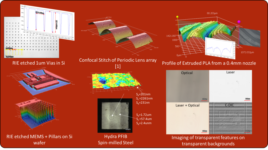
Optical Profilometry Unlimited - Keyence VK-X3050 3D Surface Profiler
The nanoFAB is pleased to announce the installation of a multi-mode Optical Profilometer from Keyence. The Keyence VK-X3050 is a red laser scanning confocal system equipped with confocal, white light interferometry (WLI), and focus variation metrology modes. The tool natively offers wide-area scanning through stitching modes. Feature-aligned, repetitive, and correlative multi-objective multi-mode measurements are enabled through user-defined Teaching modes.
100x100mm automated stage supporting up to 4" Wafers'
Through film laser thickness measurements (>1um)
Resolution:
The three analysis modes support a scaled level of resolution and accuracy. Users can combine any of the three modes to support analysis needs down to 1nm Z-resolution in Confocal and Focus Variation modes, and 0.01nm Z-resolution in WLI mode.
Laser Scanning Profilometry
The system is equipped with a high-resolution 16-bit photomultiplier that enables deep feature extraction of hard-to-analyze features such as 1µm Silicon vias. The system has demonstrated 30µm of depth resolution in narrow/confined grooves in some applications. Leveraging the high-resolution measurement capability, the automated XY stage (100mm x 100mm) allows for larger-scale analysis using single or multiple objectives. The automated measurement allows for stitching of large area samples with spatially separate or continuous features. Beyond the profilometry capabilities, optical observation can be supported, coupled, and enhanced by the laser observation modes, enabling transparent feature on transparent substrate imaging.
The Keyence VK-X3050 features a red laser diode and has demonstrated high performance imaging on high aspect ratio etched silicon, transparent bulk materials [1], 3D printed plastics, ion polished steels, and finding pesky transparent features on transparent substrates. [1] Lens array provided by Avalon Holographics as part of their 3D holographic display system
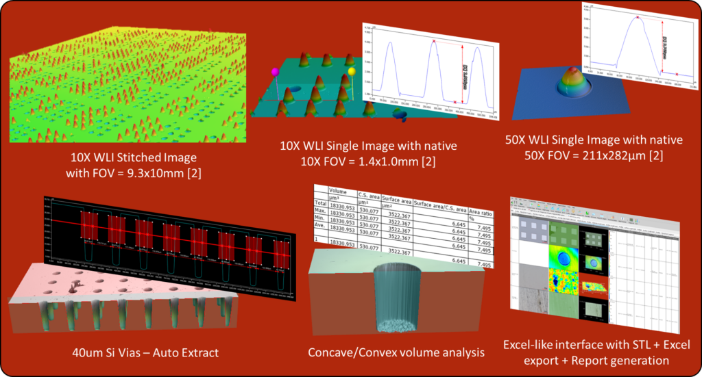
White Light Interferometry and Analysis software
In cases where Confocal microscopy fails to resolve features, the WLI mode acts not only as a complement but also as an enhancement. The WLI mode allows users to level samples through intelligent tip-tilt alignment with guided steps to achieve high-resolution measurements. The resulting files can be analyzed in the same browser as the laser confocal modes and are easily tracked by utilizing the built-in measurement metadata.
The Keyence system is equipped with white-light interferometry for high-resolution tasks and can measure transparent lens arrays [2] at 10/20/50X magnifications with native and ultra-wide FOVs. Dynamic software allows for automated feature measurements and volumetric analysis, and includes a user-friendly Excel-like interface for demanding tasks. [2] Optomechanical sensors arrays are provided by Kyle Scheuer from Ultracoustics Technologies LTD
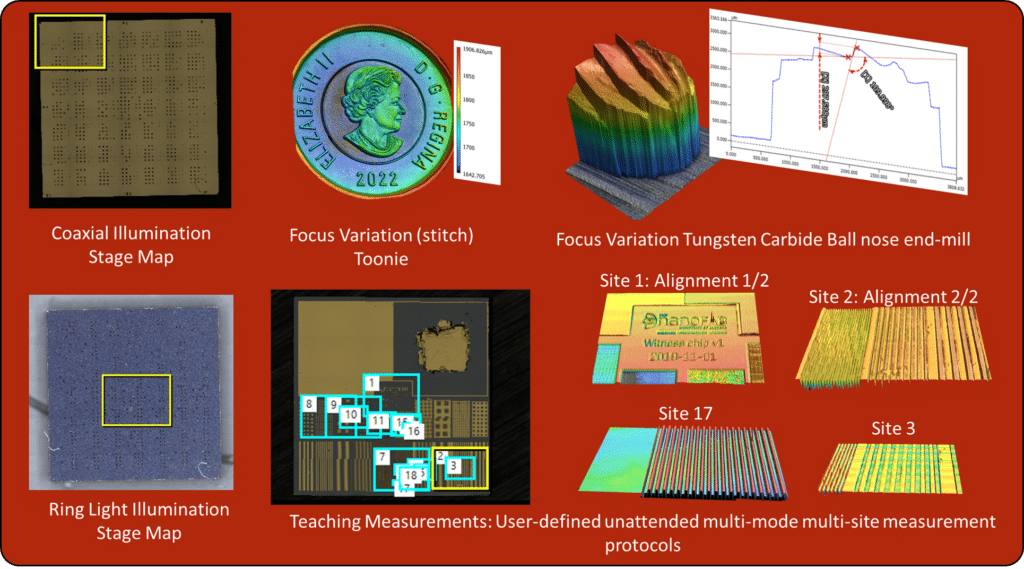
Focus variation profilometry and Teaching Modes
The system features a built-in sample mapping mode that supports any objective and allows mapping in laser and optical observation modes. Defect inspection is achievable through this feature mapping by ring-light illumination, allowing for highlighting of defect locations. The Coaxial/Ring light modes are supported by a Focus Variation Profilometry technique, enabling fast measurement of millimeter-scale features of bulk metals, coins, and machined parts. Any of the three modes, techniques, or setups can be further enhanced by the Teaching Measurement mode. Teaching Measurement modes allow for multi-mode, multi-objective, multi-site analysis that can be feature aligned across multiple runs or iterations performed today, or tomorrow.
Unique to this platform is coaxial and ring light illumination, useful for general microscopy and defect inspection. In cases of extreme feature sizes (mm scale) Focus variation techniques allow for measurement of diffusive or irregular bulk samples. The system couples these modes into an unattended automation (Teaching Mode), defined by users to allow for automatic multi-objective, multi-technique measurements at the click of a button.
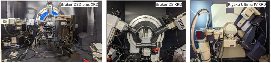
Advanced XRD techniques and applications on Bruker D8D plus diffractometer
The nanoFAB is pleased to announce that advanced In-Plane Diffraction (Non-Coplanar Scan), Pole Figure Measurement, 2D Stress Measurement, and Multi-Angle Scattering (SAXS/WAXS) are fully commissioned on the Bruker D8 DISCOVER Plus X-Ray Diffractometer .
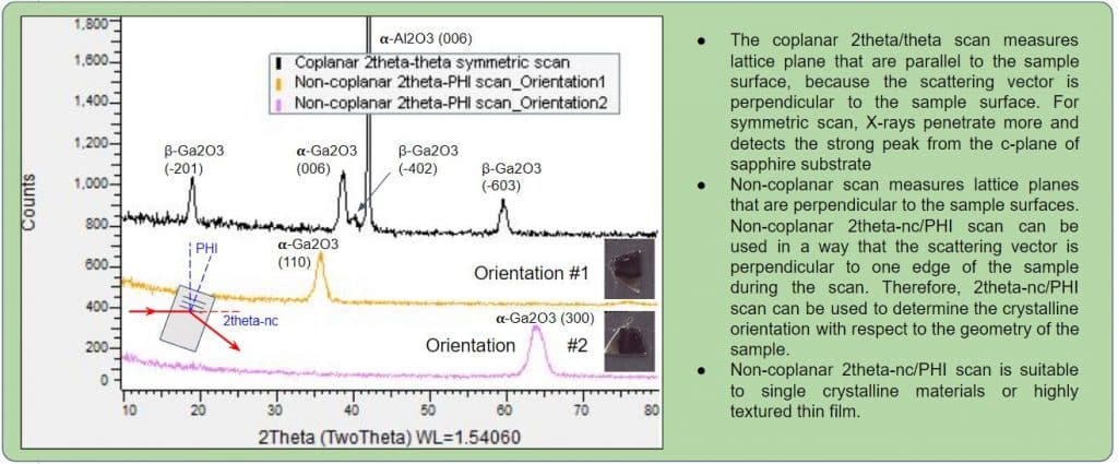
IN-PLANE DIFFRACTION (NON-COPLANAR SCAN): With standard diffraction geometries (coplanar scan), such as the Bragg-Brentano geometry, X-rays penetrate to a certain depth into the sample, and the diffraction from lattice planes parallel to the sample surface is measured. In case of ultra-thin films, X-rays completely transmit and no diffraction is observed from the thin film with the standard coplanar scan. In these circumstances, in-plane diffraction enabled by non-coplanar scan provides effective and efficient analysis, in which both the incident and diffracted beams are nearly parallel to the sample surface, as the detector scans in the plane of the horizontally positioned sample. In-plane diffraction has two major features:
(1) The penetration depth of the X-ray is limited to the top surface of the sample. By setting the X-ray incidence at the critical angle or slightly higher, ultra–thin films and the texture of surface layers can be analyzed.
(2) The technique measures lattice planes that are (nearly) perpendicular to the sample surface, which are inaccessible by other techniques. This second feature is a key difference between the in-plane grazing incidence diffraction (IP-GID) vs. the conventional GID with coplanar scan. Figure 1 shows the setup of in-plane diffraction (non-coplanar scan) on the Bruker D8D plus XRD, as compared to coplanar symmetric 2theta/theta scan for powder diffraction on the Bruker D8 XRD and coplanar GID for thin-film applications on the Rigaku XRD.
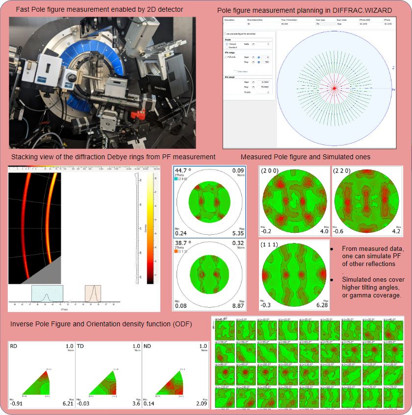
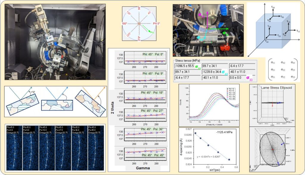
QUANTITATIVE TEXTURE ANALYSIS: The presence of crystallographic texture (preferred orientation) in polycrystalline materials has a significant effect on the anisotropy of the materials properties. Therefore, it is critically important to obtain a qualitative/quantitative description of the orientation distribution of crystallites, or the orientation distribution function (ODF) in order to characterize and predict their properties. While direct measurement of the ODF is very challenging, pole figures (PF) can be measured to reconstruct the ODF experimentally, where the diffraction angle is fixed and the diffracted intensity of a certain lattice plane is record by varying two geometrical parameters, such as the alpha angle (tilt angle of the scattering vector from the surface normal direction of a sample) and the beta angle (rotation angle of the scattering vector around the surface normal direction of a sample). The sensitive and large size 2D detector available on the Bruker D8D plus provides large coverage in Gamma and 2Theta, thus high speed and high throughput PF measurement (compared to measurement using a 0D or 1D detector), by taking 2D frames as continuous scans in PHI (the azimuthal angle) at successive values of Psi (the tilt angle).
RESIDUAL STRESS ANALYSIS: Residual stress, created during the materials manufacturing process or accumulated during operation, can have serious negative effects on a product's quality, performance, and durability, as it may result in cracks and delamination of the films, as well as deformation of the substrate depending on the adhesion strength between the film and the substrate. Residual stress X-ray diffraction is one of the techniques for evaluating the near-surface residual stress with high accuracy, which is non-destructive and is applicable to polycrystalline materials with moderate to fine grain sizes. In X-ray diffraction residual stress measurement, the strain in the crystal lattice is measured using the changes in the d-spacing of the crystal lattice planes as the strain gauge, and the residual stress producing the strain is calculated assuming a linear elastic distortion of the crystal lattice. The most commonly used method for XRD stress determination is the sin2(Psi) method. By measuring the change in the d-spacing of a suitable lattice plane for at least two different tilting angles (Psi), the stress present in the plane of sample surface can be calculated from the slope of the d vs. sin2(Psi) plot. Our Bruker D8D plus XRD provides 2D stress measurement with the side inclination method, enabled by Psi tilt and PHI rotation of the Eulerian cradle, together with the large Gamma coverage of the 2D detector. 2D stress analysis measures not only the peak position but also the shape of the diffraction Debye rings. Essentially, it describes the curvature of the diffraction rings as the scattering vector tilted away from the surface normal, providing a more generalization solution than the simple sin2(Psi) peak position analysis, which is a special condition of the 2D stress analysis. The procedure of 2D stress measurement is similar to that of 2D pole figure measurement, except that a higher-angle diffraction peak needs to be used.
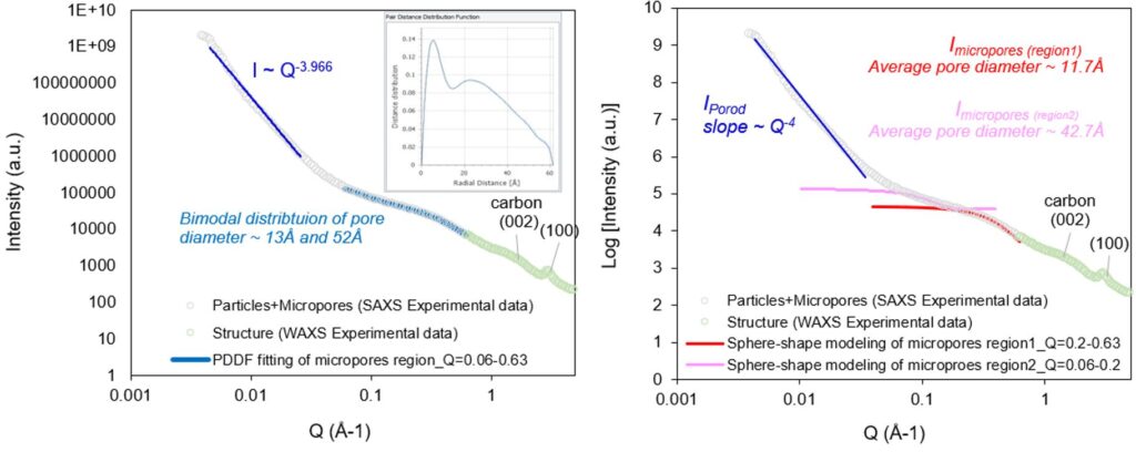
MULTI-ANGLE SCATTERING (SAXS/WAXS) ANALYSIS: Small-Angle X-ray Scattering (SAXS) analyzes the elastic scattering behavior of X-rays when traveling through the material, recording their scattering at small angles (typically 0.1 - 10°). SAXS quantifies nano-scale density differences in a sample, enabling characterization of particle sizes, shapes, distribution, pore sizes, characteristic distances of partially ordered materials, and much more. Wide-Angle X-ray Scattering (WAXS) is similar to SAXS, except that the distance from sample to the detector is shorter and thus diffraction maxima at larger angles are observed. WAXS usually covers 2theta 5-60 degree, revealing scattering/diffraction at sub-nanometer scale such as crystalline lattice planes. Multi-angle scattering analysis utilizes both SAXS and WAXS in conjunction to probe a wide range of length scale from an angstrom to a micrometer, revealing a full picture of the materials structure.
In-plane diffraction, pole figure, and 2D stress measurements are now available for user training and staff analysis. Please see the application examples and discussions below for more details. If you are interested in utilizing these techniques for your materials characterization, please submit a training request on LMACS. If you have any questions, please feel free to contact Dr. Xuehai Tan (xtan@ualberta.ca) and Peng Li (peng.Li@ualberta.ca) – the Characterization Group Manager.
Figure 1 - Comparison of non-coplanar scan, coplanar symmetric scan, and coplanar GID scan setups on nanoFAB XRD systems.
Application Examples
Sample: Epitaxially grown Ga2O3 thin film on sapphire substrate Analysis: In-plane diffraction (Non-coplanar scan) Application: Coupling non-coplanar 2theta-nc / PHI scan and coplanar 2theta/theta symmetric scan to characterize epitaxially grown Ga2O3 thin film on sapphire substrate.
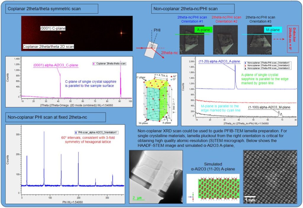
Sample: Single crystal sapphire α-Al2O3 Analysis: In-plane diffraction (Non-coplanar scan) Application: Coupling different non-coplanar scans and coplanar symmetric scan to characterize single crystalline materials. An example is given on how in-plane diffraction could be used to guide PFIB-TEM lamella preparation.
Sample: Soda can Al sheet produced through cold-rolling Analysis: Fast pole figure measurement enabled by 2D detector Application: Texture analysis of the orientation distribution of crystallites from pole figure measurements.
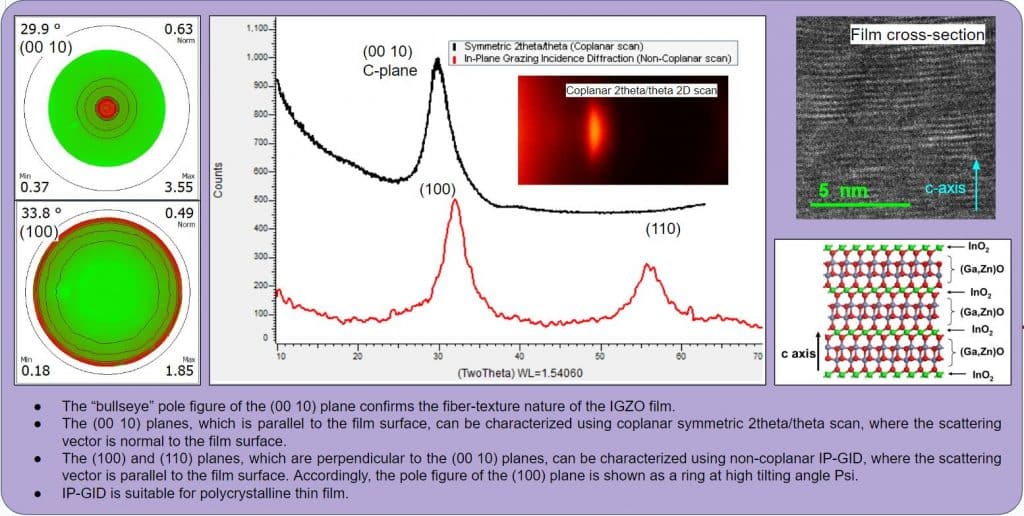
Sample: Fiber-textured In-Ga-Zn-O (CAAC-IGZO) film on Si substrate for 3D glasses-free holographic displays Analysis: Pole figure, coplanar symmetric scan, non-coplanar in-plane GID, PIB-STEM Application: A correlative study of fiber-textured IGZO film using pole figure, coplanar and non-coplanar XRD (In-plane GID), and PFIB-STEM microscopy of the film cross section. Sample Courtesy:Avalon Holographics Inc., Edmonton
Sample: Fe film with compressive stress Analysis: 2D stress analysis Application: A more generalization residual stress analysis solution than the simple sin2(Psi) peak position analysis
Sample: A hard carbon with rich closed pores. Analysis: Multi-angle X-ray scattering Application: Coupling SAXS and WAXS to investigate the internal pore sizes and the short-range ordered carbon structure.
Correlative imaging workflow available on SEM/FIB
Electron & Ion Microscopy (SEM, FIB and TEM) provides morphological and compositional analysis with ultra high spatial resolution but lack of larger macroscopic context. It is also challenging to obtain analysis and observations with multiple sources from identical locations of the same devices/samples, in order to obtain comprehensive data.
Software solutions are now installed and commissioned in the following microscopes, providing large area imaging and correlative workflow:
ATLAS on Zeiss Sigma FESEM ATLAS on Zeiss EVO SEM MAPS on ThermoFisher Hydra Plasma FIB/SEM
These software packages enable automatic workflow of multi-scale (from cm to nm), multi-platform (optical, x-ray, electron and ion microscopy and spectroscopy) and multi-dimensional (2D, 3D and 4D) characterization. Please see the application examples below of how the workflow can provide correlative analysis by linking Optical, Raman, AFM, XRM, SEM, FIB, and TEM data.
ATLAS and MAPS software are now available for user training. If you are interested in utilizing the workflow for your material characterization, please submit a training request on LMACS. If you have any questions, please feel free to contact Shihong Xu (shihongx@ualberta.ca), Josh Perkin (jperkins@ualberta.ca) or Peng Li (peng.li@ualberta.ca).
Application Examples
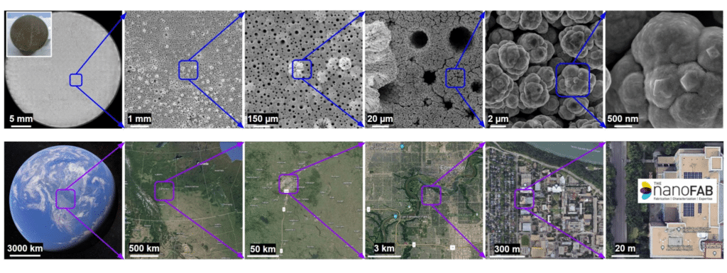
Sample: Porous Ni film Application: Large area imaging for multi-scale analysis (Google Earth like images with high spatial resolution) Instrument: Zeiss Sigma FESEM
A series of images seamlessly integrates correlative imaging to showcase a progressively zoomed view from a large object to a microscopic structure, transitioning from a satellite view of Earth to the intricate details of building layouts.
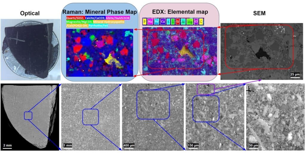
Sample: Shale Application: Multi-scale and correlative SEM/EDX/Raman analysis of elemental and mineral distribution Instruments: Zeiss EVO SEM with Oxford EDX Renishaw inVia Confocal Raman
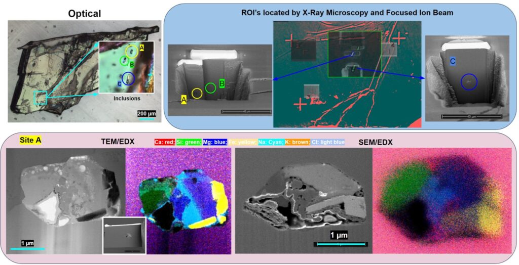
Sample: Mineral inclusions Application: Multi-scale and correlative SEM/EDX/XRM/TEM analysis of mineral inclusions in magnetite-apatite deposits This work is published in Geology (2024) 52 (6): 417–422
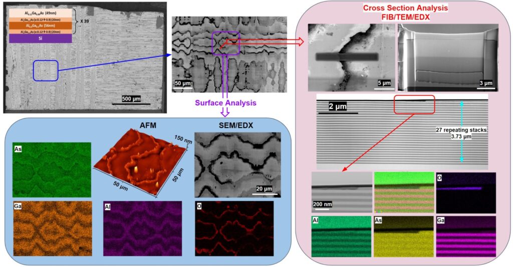
Sample: Multi-layer AlGaAs thin film Application: Correlative SEM/EDX/AFM/TEM analysis to characterize both surface and cross section morphology and composition Instruments: ThermoFisher Hydra Plasma FIB/SEM Bruker Dimension Edge AFM JEOL ARM S/TEM
Advanced TEM Sample Preparation
Focused Ion Beam (FIB) provides preparation of site-specific, high-quality S/TEM samples for a wide range of materials. Unlike the conventional Ga-FIB, which has slow milling rate, results in Ga damage/implantation, the ThermoFisher Helios Hydra Plasma FIB (equipped with multiple inert ion species - Xe and Ar) overcomes those unwanted effects and produces damage free TEM lamellas./
The latest technological innovations on the Hydra PFIB microscope, such as flexible control of micro-manipulator and stage, multi-precursor gas injection system (GIS), along with well integrated software solutions, enable fast and easy lamella preparation with high throughput for TEM analysis, less dependent on the operators’ experience.
Our Characterization team is pleased to announce that all advanced processing for TEM lamella preparation on the Hydra PFIB have been successfully commissioned, including:
Low voltage Xe and Ar beams to produce damage free samples
Micro-manipulator (EasyLift) with continuous axial rotation, enabling flexible pluckouts, such as 90-degree / inverted pluckouts for both cross-sectional and plan-view preparation.
Multiple precursors for Gas Injection System (GIS): C, Pt, W, providing flexible capping films for materials with different hardness and backfilling for porous materials.
Automatic Lamella Sample preparation: fully automatic site preparation and software-assisted pluckout and final polishing.
Our user groups have utilized those techniques to produce TEM samples for their characterization needs. If you are interested in preparing TEM lamellas on the Hydra PFIB system, user training and staff analysis are available. Please submit a request (training or sample type) with sample details on LMACS. If you have any questions, please feel free to contact Dr. Shihong Xu (shihongx@ualberta.ca) - PFIB, Xuehai Tan (xtan@ualberta.ca) - TEM or Peng Li (peng.li@ualberta.ca) – the Characterization Group Manager.
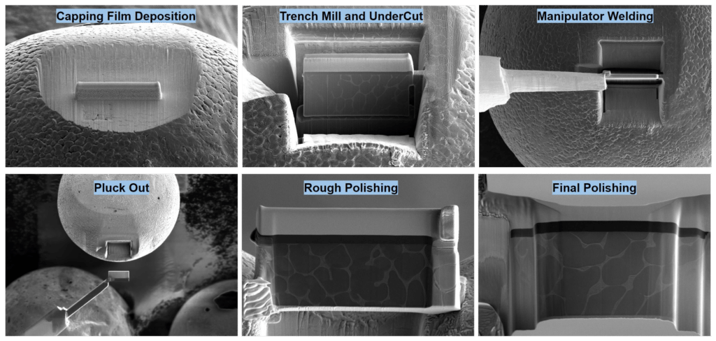
Standard Lamella Preparation
Series of six images illustrating stages in advanced TEM sample preparation: capping film deposition, trench milling and undercutting, manipulator welding, plucking out, rough polishing, and final polishing.
Application Examples
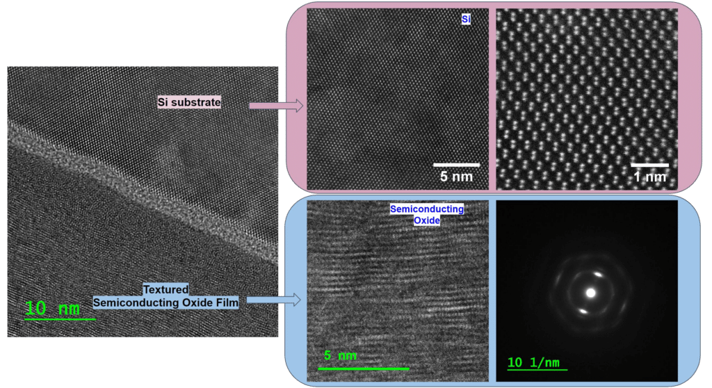
Sample: Semiconducting Oxide Film on Si FIB Application: Low voltage 2kV Ar polishing to produce damage free sample for HR-STEM imaging Sample Courtesy: Avalon Holographics Inc., Edmonton
Microscopic images reveal the Si substrate (upper panel) and a textured semiconducting oxide film (lower panel), featuring distinct nano-scale structures and electron diffraction patterns, achieved through advanced TEM sample preparation techniques.
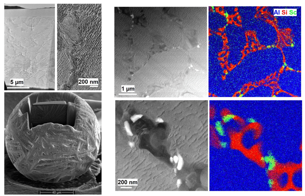
Sample: Rapidly solidified Al-10Si-0.4Sc droplets (atomized using Impulse Atomization) FIB Application: Flexible micromanipulation to pluckout samples from spheres Sample Courtesy: Akki Sahoo, Dr. Jonas Valloton and Prof. Hani Henein, Faculty of Engineering, University of Alberta; Abdoul-Aziz Bogno, Equispheres Inc., Ottawa
A collage of microscopic images, prepared with advanced TEM techniques, showcases various materials' textures and compositions with scale bars. The top right image features a color map, highlighting elements labeled as Al, Si, and Sc.
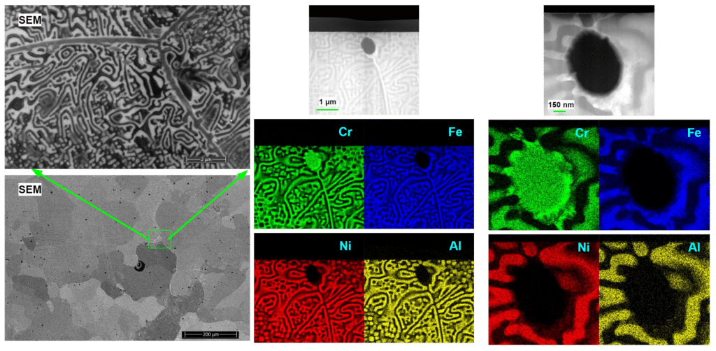
Sample: Al-Cr-Fe-Ni medium-entropy alloy (MEA) FIB Application: Mixed Pt/C capping film for effective protection for HEA/MEA materials Sample Courtesy: Guijiang Diao and Prof. Dongyang Li, Faculty of Engineering, University of Alberta
A series of SEM and color maps displaying material composition, with elements Cr (green), Fe (blue), Ni (red), Al (yellow) on a patterned surface. Focus is on a circular area, highlighting the precision in sample preparation for Advanced TEM analysis.
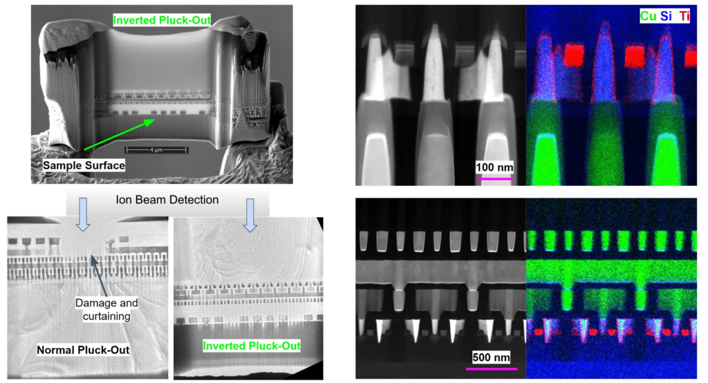
Sample: Intel Core i7 processor FIB Application: Inverted pluckout to reduce curtaining and damage in the regions of interest.
Advanced TEM images reveal semiconductor structures with ion beam detection, highlighting inverted pluck-out areas. Color coding indicates elements: Cu, Si, Ti, ensuring precise TEM sample preparation for detailed analysis.
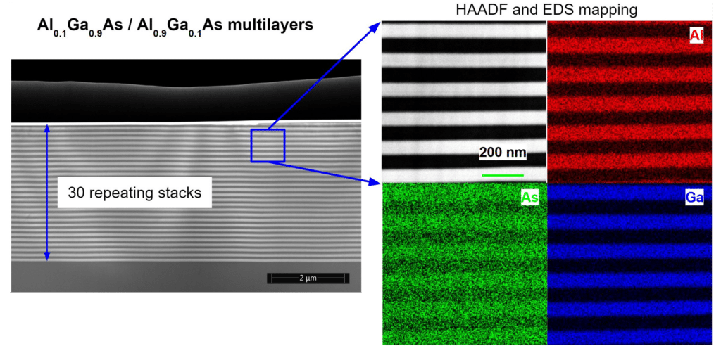
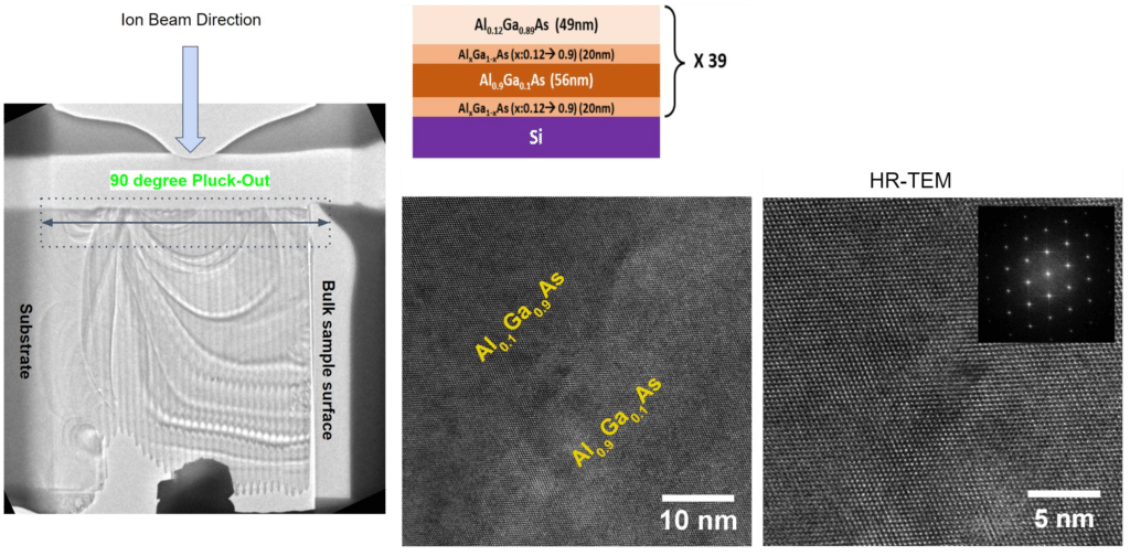
Sample: AlGaAs multilayers FIB Application: 90-degree pluckout (ion beam parallel to the layer stacks) to produce uniform thin thickness across all layers.
A semiconductor cross-section reveals layers of Al₀.₃Ga₀.₇As and Al₀.₄₅Ga₀.₅₅As on Si, with advanced TEM images and a diffraction pattern presented on the right, highlighting meticulous sample preparation techniques.Advanced TEM nanobeam diffraction images reveal crystallographic mismatch in Al[_x]Ga[_{1-x}]As/Al[_y]Ga[_{1-y}]As layers, complemented by a selected area electron diffraction pattern.Microscopic image of AlGaAs/AlGaAs multilayers displaying 30 repeating stacks. Includes HAADF and EDS mapping with highlighted elements: Al in red, As in green, Ga in blue. Advanced TEM sample preparation showcases intricate layer details for accurate analysis.
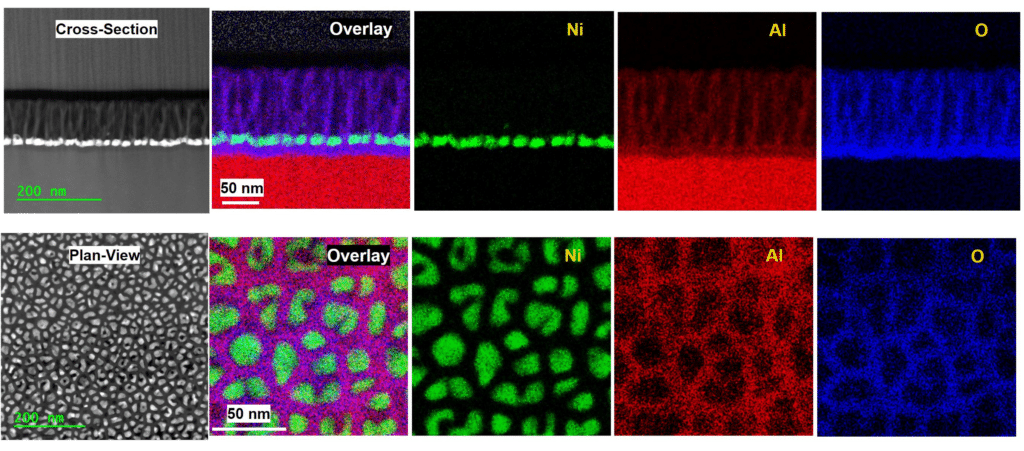
Sample: Nano-composite material (Ni nanoparticles in anodized Al) FIB Application: Flexible miro-manipulation to produce cross-sectional and plan-view lamellas Sample Courtesy: Dr. Matthew Nickel and Prof. Todd McMullen, Faculty of Medicine & Dentistry, University of Alberta
Advanced TEM cross-sectional and plan-view microscopy images reveal distributions of Ni, Al, and O with remarkable clarity. The cross-section shows stratified layers, while the plan-view features patchy clusters. Scale bars are set at 200 nm and 50 nm respectively.
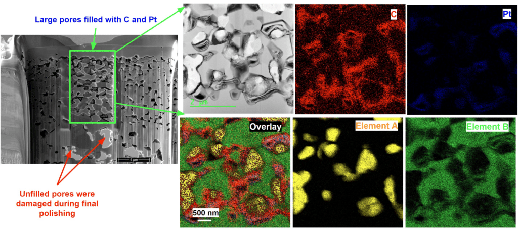
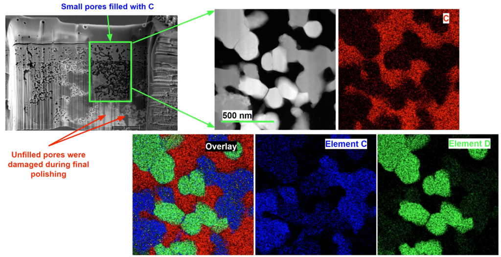
Sample: Porous solid oxide fuel cell FIB Application: Back-filling with in-situ GIS to prepare high quality samples from porous materials. Sample Courtesy: Prof. Douglas Ivey, Faculty of Engineering, University of Alberta
Microscopic images using advanced TEM reveal pores, element concentration maps, and overlays; highlighting small carbon-filled pores and unfilled, damaged pores.
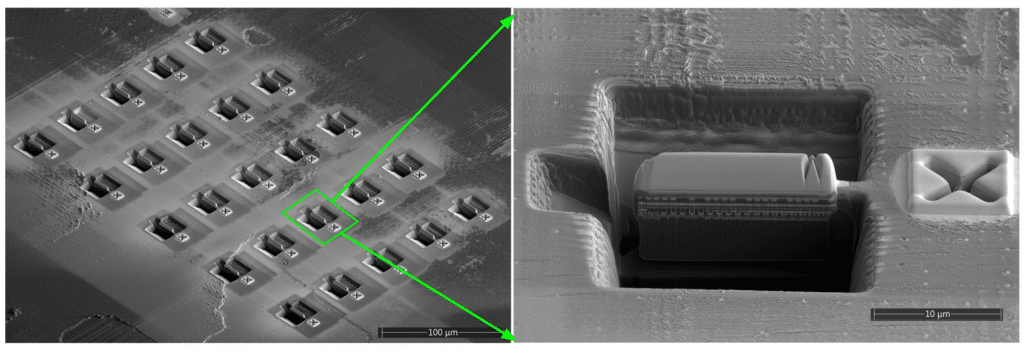
Sample: Intel Core i7 processor FIB Application: Fully automatic/unattended site preparation of 25 locations
A grayscale image showcasing a zoomed-in view of microstructures highlights an inset detailing a close-up of one microstructure, prepared using Advanced TEM techniques, featuring a rectangular shape inside a square cavity.
SAXS, GI-SAXS/WAXS are available on Bruker D8D+
The nanoFAB is pleased to announce that advanced Small-Angle X-ray Scattering (SAXS), Grazing-Incidence Small-Angle and Wide-Angle X-ray Scattering (GI-SAXS/WAXS) techniques are fully commissioned on the Bruker D8 DISCOVER Plus X-Ray Diffractometer and now open for user training.
SAXS utilizes small-angle x-ray scattering to quantify nano-scale density differences in a sample, which enables characterization of nanostructures in terms of the averaged particle sizes, shapes, distribution, pore sizes, characteristic distances of partially ordered materials, and much more. This is achieved by analyzing the elastic scattering behavior of X-rays when traveling through the material, recording their scattering at small angles (typically 0.1 - 10°).
The materials for SAXS analysis can be solid or liquid and they can contain solid, liquid or gaseous domains (so-called particles) of the same or another material in any combination. Not only particles, but also the structure of ordered systems like lamellas, and fractal-like materials can be studied. For thin films supported on solid substrates (such as glass or Si), derivatives of SAXS, namely GI-SAXS/WAXS can be used to characterize ordered structure/alignment within the films relative to the substrate surface, particularly molecular alignment/arrangement of polymer films. These methods are accurate, non-destructive and usually require a minimum of sample preparation. Applications are very broad, including colloids of all types, metals, cement, oil, polymers, plastics, proteins, foods and pharmaceuticals.
If you are interested in the SAXS, GI-SAXS/WAXS analysis, please submit a request (training or sample type) with sample details on LMACS. Our XRD team (Drs. Xuehai Tan and Nas Yousefi) will follow up and arrange sample analysis and training. If you have any questions, please feel free to contact Peng Li (Peng.Li@ualberta.ca) – the Characterization Group Manager.
Application Examples
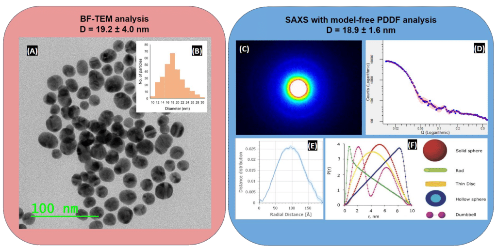
Sample: 20 nm Au NPs Sample preparation: in water (capillary tube) Analysis: SAXS Application: Size distribution analysis
Among several techniques to measure particle size, SAXS provides accurate, reliable and high throughput analysis with simple sample preparation. While TEM imaging based analysis provides direct visualization with very high spatial resolution, it requires proper sample preparation (well dispersed particles) and the result accuracy relies on the quality of particle intensity thresholding. SAXS analysis is less dependent on sample preparation and probes a large volume of samples, providing the most statistically relevant results.
Figure 1: (A) Bright-Field TEM image and (B) measured size distribution of the Au nanoparticles, diameter = 19.2 ± 4.0 nm. (C) 2D SAXS data measured with an evacuated flight tube (EFT) filled with vacuum. (D, E) SAXS data integrated into 1D and background subtraction: A model-free analysis based on Pair Distance Distribution Function (PDDF). The obtained result is indicative of an overall spherical particle shape with approximated diameter of 18.9 nm. (F) PDDF P(r) functions for geometric bodies, adapted from DOI 10.1088/0034-4885/66/10/R05
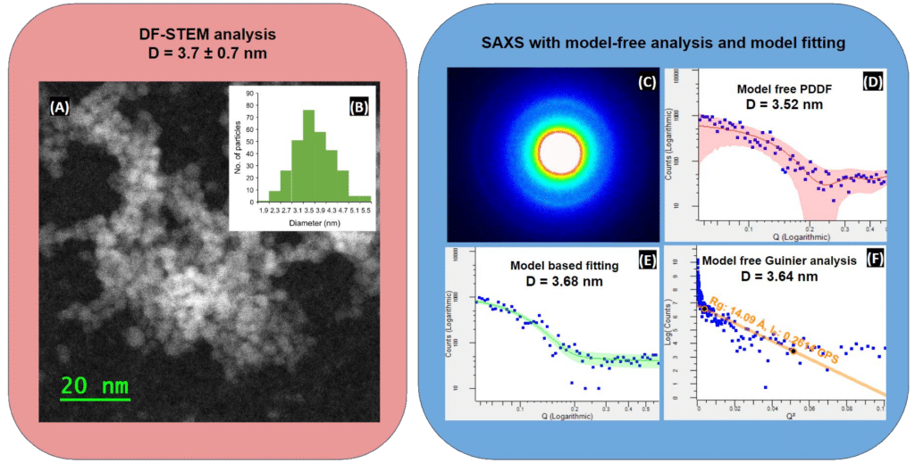
Sample: 3 nm Si QDs Sample preparation: in toluene (capillary tube) Analysis: SAXS Application: Size distribution analysis Sample Courtesy: Chuyi Ni and Prof. Jon Veinot, Department of Chemistry, University of Alberta
TEM imaging analysis can be very challenging to characterize particle size when particles are difficult to disperse and/or the particles give poor contrast, such as light-element quantum dots (QDs), e.g., Si or carbon QDs. SAXS can provide reliable size and shape structure determination, empowered by several data analysis / modelling methods and further advances in instrumentation.
Figure 2: (A) Dark-Field STEM image and (B) measured size distribution of Si QDs, diameter = 3.7 ± 0.7 nm. (C) 2D SAXS data measured with an evacuated flight tube (ETF) filled with vacuum. SAXS analysis results with model free and model fitting: (D) Model free PDDF, diameter = 3.52 nm; (E) a model-based fitting assuming polydisperse spheres with Schultz size distribution and no interaction, diameter = 3.68 nm; (F) model-free Guinier analysis, diameter = 3.64 nm.
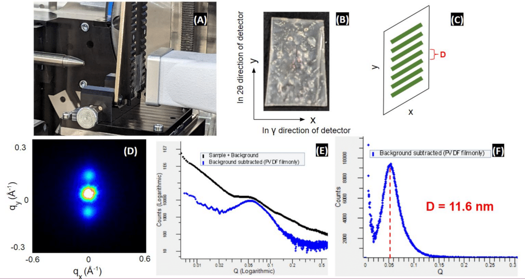
Sample: textured PVDF film Sample preparation: Freestanding film Analysis: SAXS Application: Internal periodical structures and orientation Sample Courtesy: Amanuel Abay and Prof. Anastasia Elias, Faculty of Engineering, University of Alberta
SAXS is useful not only for characterizing the size and shape of particles, but also for measuring structural information of partially or completely disordered systems. In the following example, SAXS analysis is utilized to study the internal repeating structure of a free-standing PVDF film.
Figure 3: (A) a photo of the SAXS setup, including X-ray collimator, the vertically mounted free-standing PVDF film, and the evacuated flight tube (EFT) that is attached to the 2D detector. (B) The orientation of the sample with respect to the 2theta and gamma directions of the 2D detector. (C) Illustration of the internal lamella orientation confirmed by the SAXS analysis. (D) 2D SAXS data marked with q values in both 2𝛉 and 𝞬 directions. (E) SAXS data integrated into 1D and background subtraction. (F) The measured q value suggests a repeated distance of 11.6 nm for the internal lamella.
Sample: Organic Photovoltaic (OPV) films (30 nm PEDOT + 250 nm P3HT:PCBM) Sample preparation: Spin-coated on ITO-coated glass substrate Analysis: GI-SAXS Application: Internal periodical structures and orientation Sample Courtesy: Prof. Jillian Buriak, Department of Chemistry, University of Alberta
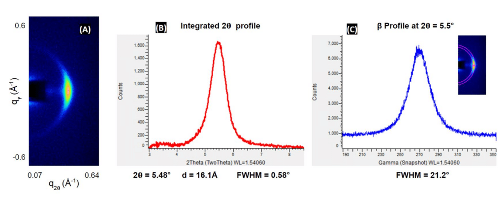
GI-SAXS is particularly useful to analyze domain size, interplanar spacings and orientation of small molecule/polymer thin films for photovoltaics, block copolymer thin films and inorganic/metal thin films for batteries. GI-SAXS analysis of an organic Photovoltaic film (P3HT:PCBM) measured an interplanar spacing d = 1.61 nm and their 2D distribution (both in-plane 2𝛉 and out-of-plan β).
Figure 4: (A) 2D GI-SAXS data marked with q values in both 2𝛉 and gamma directions; (B) Integrated profile in 2𝛉 direction and (C) Integrated profile in β direction.
Sample: PBTTT film (30 nm) Sample preparation: spin-coated on ITO-coated glass substrate Analysis: GI-WAXS Application: Internal periodical structures and orientation Sample Courtesy: Prof. Loren Kaake, Department of Chemistry, Simon Fraser University
Semiconducting polymers play an important role in advancing the field of printed and mechanically flexible electronics, such as flat panel displays and photovoltaic cells. Thin film transistors with thiophene-based polymer layers have demonstrated good field-effect carrier mobilities that are considered highly valuable across various applications. It is widely recognized that achieving high carrier mobility in these materials hinges on the precise molecular ordering, as charge movement depends on effective intermolecular electronic coupling. While the spacing of the molecular ordering and crystalline domains is too small for GI-SAXS, GI-WAXS provides an effective analysis.
As shown in the figures below, typical GI-WAXS setups on the Bruker D8D plus (0.1 mm slit and a 0.3 mm Goebel mirror collimator, 0.17° incidence angle, and 145 mm sample-to-detector distance) effectively confirms the edge-on orientation of the polymer lamellas in a 30 nm PBTTT film on glass.
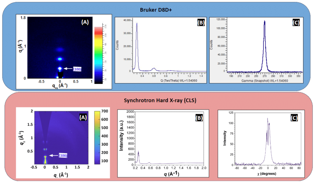
Compared to the results (available here) obtained from the Synchrotron Hard X-ray MicroAnalysis (HXMA) beamline (at the Canadian Light Source), the GI-WAXS analysis on the Bruker D8D plus provides equally informative results, but more accessible to general users.
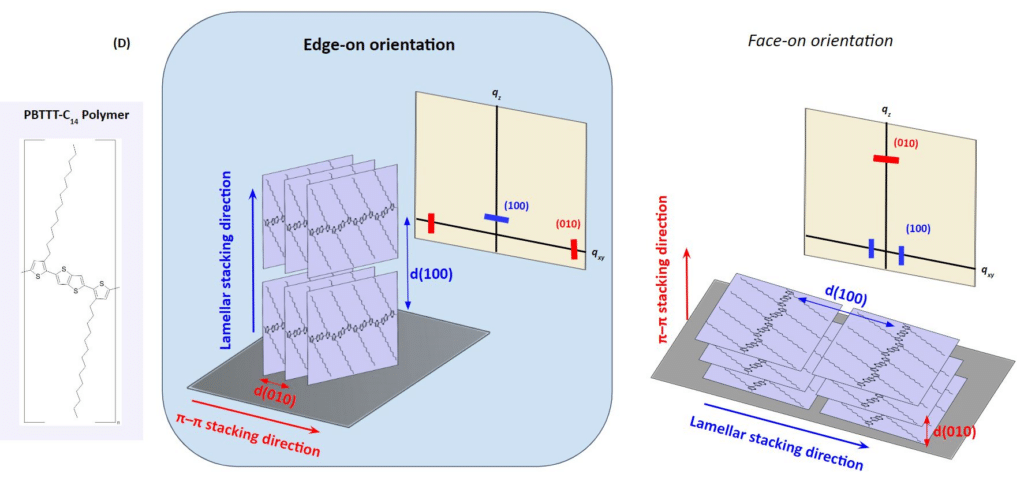
Figure 5: GI-WAXS results of PBTTT thin films measured on the Bruker D8D + and the Synchrotron Hard X-ray MicroAnalysis (HXMA) beamline of the Canadian Light Source. (A) Two-dimensional WAXS scattering data (B) 1D profile of the scattering intensity. (C) Azimuthal dependence of the scattering intensity. (D) The molecular structure of PBTTT and the schematic depicting PBTTT different molecular alignment within thin layers relative to the substrate surface: Edge-On and Face-On orientations. The arrangement of molecules within the cell is primarily qualitative and is not intended to provide a quantitative representation of the precise molecular packing specifics.
Broad Ion Beam (BIB) polishing for SEM/EDX/EBSD
The RES 102 system features:
Ion energy: 0.8 to 10 keV
Source current: Up to 4.5 mA
Stage Rotation: 0.6 to 10 rpm
Sample size SEM holder: max. Ø 25 mm × 12 mm
Prepared area SEM holder: max. Ø 25 mm
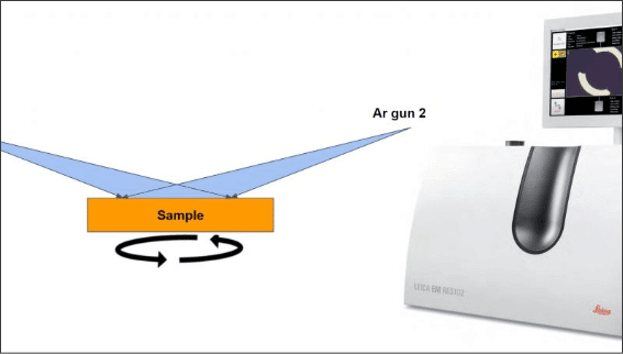
RES102 BIB Ion Milling System equipped with two Ar guns
Among general electron microscopy applications, Electron Backscatter Diffraction (EBSD) is a surface technique – typical probing depth is in the range of a few tens nm for a beam energy of 20 kV. Smooth and damage-free surface is critically important to obtain high quality EBSD data. Compared to conventional mechanical polishing techniques, which can result in very rough surfaces and a thick damaged layer, low energy beam at grazing incident angle and rotating stage on the RES102 can effectively polish the surface to reduce roughness and remove the damaged layer.
With the programmable recipes of flexible parameters (beam energy, beam current, incident angle, stage rotating speed), the RES102 BIB has produced very nice results for our users for EBSD analysis. See recent examples below.
Application Examples (EBSD)
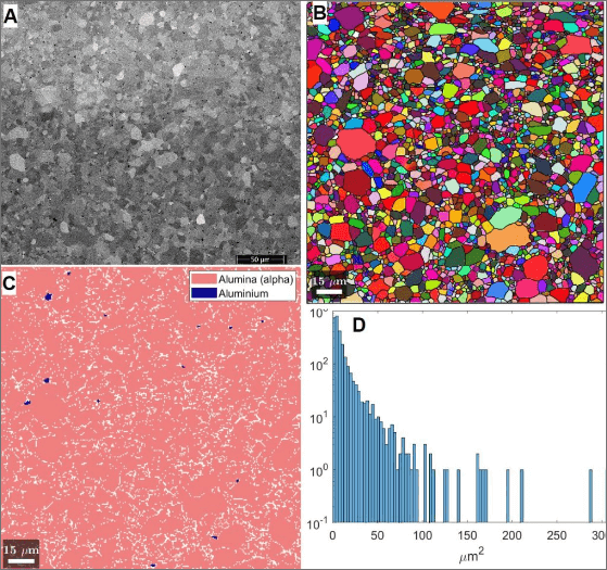
Sample: 3D printed Alumina for structural applications
Sample Courtesy: Cass (Haoyang) Li, Dr. James Hogan, Mechanical Engineering Department, Faculty of Engineering, University of Alberta
Ion Milling process:
8 kV, 3 mA, 3.5 degrees, 1.5 rmp for 120 mins
8 kV, 2 mA, 2.5 degrees, 1.5 rmp for 60 mins
EBSD mapping: 175 µm x 175 µm, stepsize 50 nm
(A) SEM image; (B) Orientation map; (C) Phase maps of Alumina and Aluminium; (D) Grain size distribution
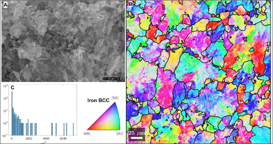
Sample: Rail Steel
Sample Courtesy: Stephen Okocha, Drs. Ben Jar and Michael Hendry, Mechanical Engineering Department, Civil and Environmental Engineering Department, Faculty of Engineering, University of Alberta
Ion Milling process:
8 kV, 3 mA, 2.5 degrees, 1.5 rmp for 60 mins
6 kV, 2 mA, 2.5 degrees, 1.5 rmp for 60 mins
EBSD mapping: 300 µm x 300 µm, stepsize 250 nm
(A) SEM image; (B) Orientation map; (C) Grain size distribution
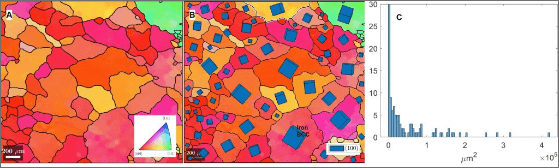
Sample: Al-Cr-Fe-Ni medium-entropy alloy (MEA)
Sample Courtesy: Guijiang Diao, Dr. Dongyang Li, Chemical and Materials Engineering Department, Faculty of Engineering, University of Alberta
Ion Milling process:
8 kV, 3 mA, 3.5 degrees, 1.5 rmp for 60 mins
5 kV, 2 mA, 2.5 degrees, 1.5 rmp for 60 mins
EBSD mapping: 2500 µm x 1500 µm, stepsize 500 nm
(A) Orientation map; (B) Crystal unit cell orientation and (C) Grain Size Distribution
The RES102 ion milling system is now available to general users for both staff analysis and user training. Any users interested in getting trained on this tool or staff analysis should submit a request on LMACS. If you have any questions, please contact the tool managers Drs. Nas Yousefi and Shihong Xu or Peng Li – the Characterization Group Manager
![Advanced TEM nanobeam diffraction images reveal crystallographic mismatch in Al[_x]Ga[_{1-x}]As/Al[_y]Ga[_{1-y}]As layers, complemented by a selected area electron diffraction pattern.](https://www.nanofab.ualberta.ca/wp-content/uploads/2025/02/06b-Al-Ga-As-1024x410.png)