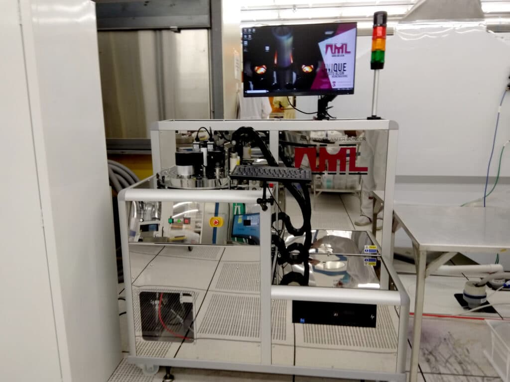
AML Wafer Bonder now available for training

The nanoFAB is pleased to announce an upgrade to our wafer bonding and packaging area, with the recent installation of a wafer bonder from Applied Microengineering Ltd (AML).  The AWB-04 wafer aligner-bonder from AML offers a wide range of bonding techniques and process flexibility. Of particular note is its in situ alignment capability, allowing users to verify correct alignment as the wafers are being brought into contact.


Bonding techniques include:

Technical features:


Application Examples

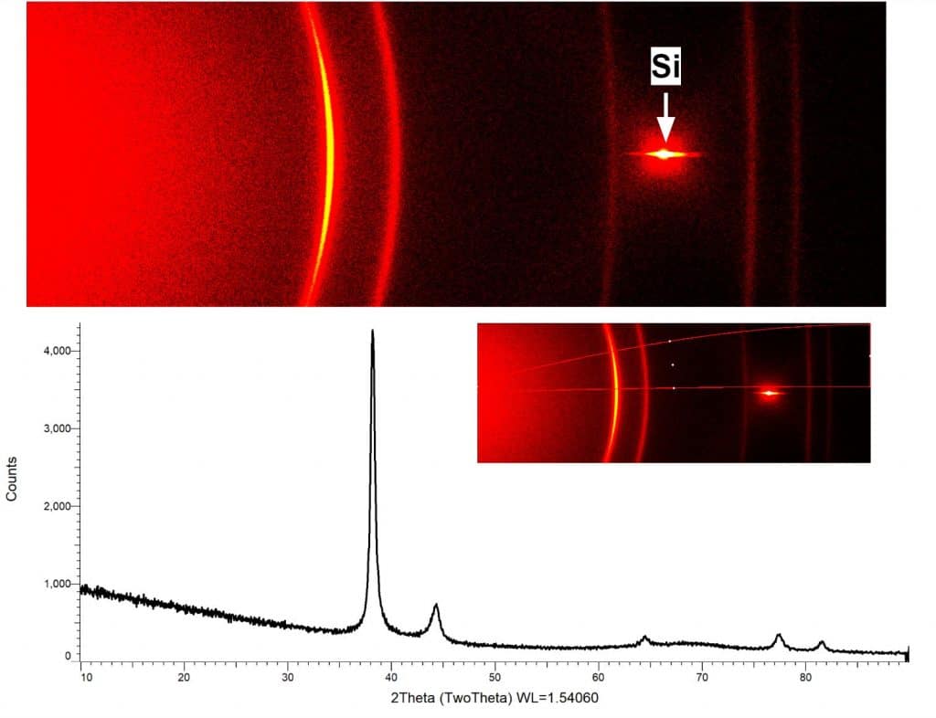
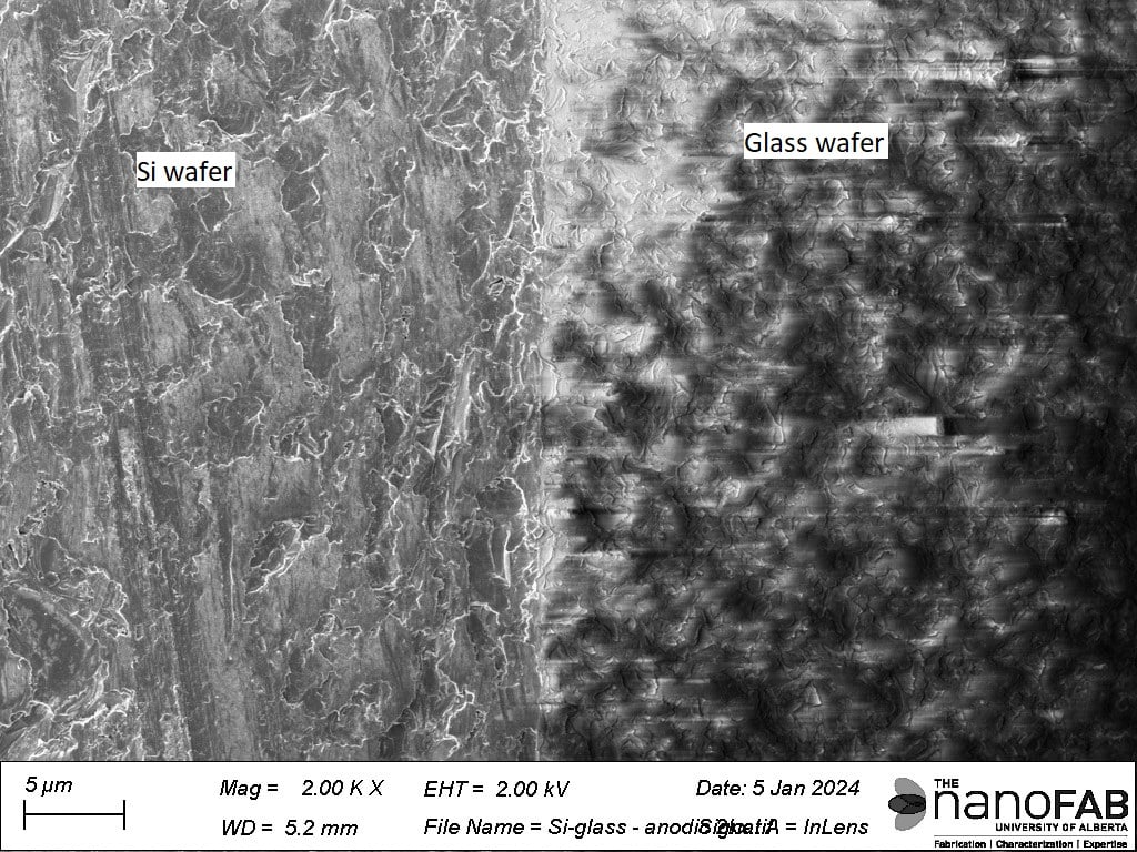
Anodic Bond: borosilicate glass to Si

Cross-sectional SEM (left) and TEM (right) images of bonding interface.

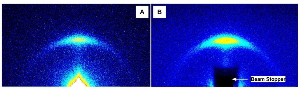
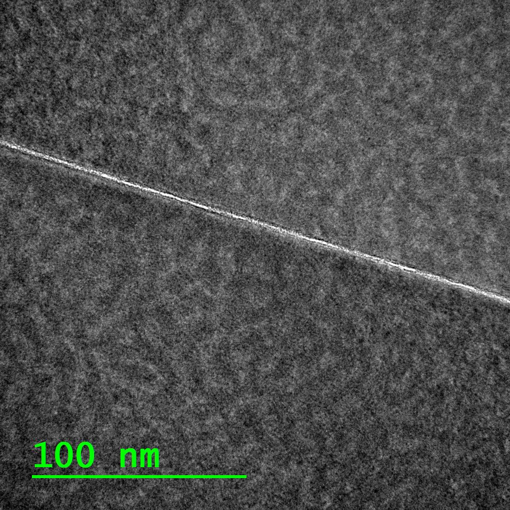
Si–Si Direct Bond: in situ RAD + low-temperature anneal

TEM images of the bonding interfaces of silicon wafers after a low-temperature (250 °C) anneal performed in the AWB-04 chamber without breaking vacuum. The thin amorphous native SiO2 layer can be seen along the interface.

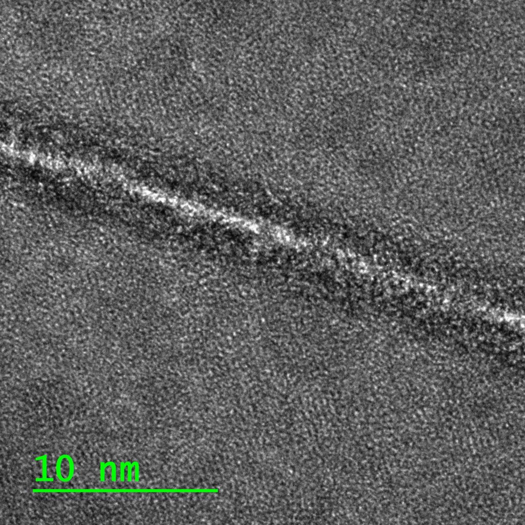
Si–Si Direct Bond: in situ RAD + external high-temperature anneal

TEM images of the bonding interfaces of silicon wafers after a high-temperature (1100 °C) anneal performed in Tystar General Anneal (Tube 6). The thin amorphous native SiO2 layer can be seen along the interface, but has diffused into the bulk Si layer.

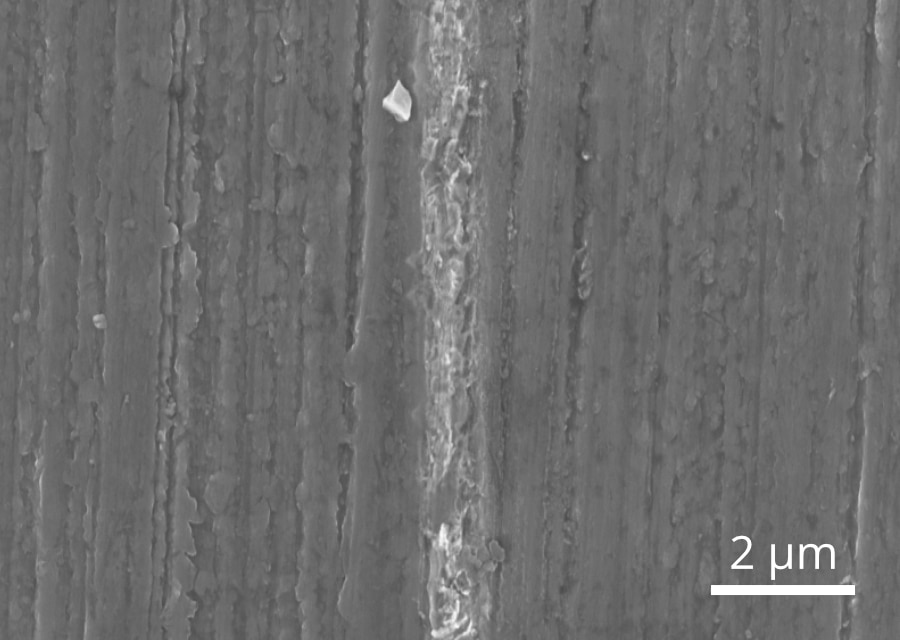
Au–Au Thermocompression Bond: Si to Si with Au interlayers

SEM images of silicon wafers bonded via Au–Au thermocompression bonding: full wafer cross-section (left) and close-up of bond interface (right). Patterned Au films are deposited on Si wafers and bonded using moderate temperatures (~300 °C) and high pressures (~7.5 MPa). Images courtesy of Jones Microwave Inc. and RM3.

If you are interested in using the AML wafer bonder in your work, please submit a request through LMACS to receive training. If you have any questions, please feel free to contact Scott Munro or Aaron Hryciw.

New Spray Coating Tool Available

We are happy to announce a new addition to our fabrication tool lineup: a Sono-Tek ExactaCoat Spray Coater. This tool is located in our recently renovated 10k Lithography area (ECERF W1-031); please stay tuned over the coming months as we add more photolithography capabilities to this labspace.

The ExactaCoat, an ultrasonic spray coating system, can accommodate specimens up to 300 mm in diameter. This tool is primarily used for photoresist coating in situations where conventional spin coating is impractical or yields poor results: specimens that are too fragile, exhibit large topographical variations, or possess irregular shapes.

The spray coater offers a particular advantage for specimens where topography presents a challenge to achieving good film uniformity during spin coating: examples include MEMS or microfluidic devices with deep (tens to hundreds of µm) features etched via DRIE or KOH/TMAH. Process development is currently underway to formulate recipes suitable for coating deep and/or high aspect ratio topography wafers. Additionally, spray coating is a valuable technique for those looking to apply photoresist as a dicing protect layer on extremely fragile or through-etched substrates that are not compatible with spin coating.

Sono-Tek ExactaCoat Spray Coater
Illustration depicting stages of droplet formation: solvent evaporation in flight, landing on a substrate, and forming a closed resist film, annotated with arrows and text labels. The spray coating process is enhanced with our Spray Coating Tool available for precision applications.
Schematics of the spray coating process
(MicroChemicals)

The spray coating process uses high-frequency (ultrasonic) mechanical vibration that is transferred to the liquid in the nozzle. The standing waves created in the liquid are broken up as the liquid exits the nozzle—this aerosolised liquid is then dispensed onto the surface of the specimen as a fine mist.

 
To coat an extended specimen such as a wafer, the spray of atomised resist is rastered across the work area in overlapping stripes. This is illustrated in the following videos, where a cleanroom wipe is used to show the sprayed resist more clearly.

After spray coating a wafer with resist and softbaking, it may be exposed and developed to complete a photolithography process. The following optical microscope images illustrate some preliminary results of photolithography on Si wafers, showcasing excellent film uniformity and achieving lateral feature sizes as small as 5 µm.

Photolithography using spray coating: Si wafers spray coated with a ~4.5 µm thick film of AZ 1505, exposed in a contact mask aligner, and developed. The smallest feature size pictured in each image is 5 µm.

We are thrilled to introduce this new capability, along with the array of associated applications it makes possible. If spray coating is a technique you feel would be beneficial to your work, please submit a request through LMACS to receive training. If you have any questions, please do not hesitate to contact Breanna Cherkawski or Aaron Hryciw.

Resources

Application note: Spray coating (MicroChemicals GmbH)

Raith_GDSII toolbox documentation now on Read The Docs

Now in its tenth year of existence, the Raith_GDSII MATLAB toolbox makes it easy to generate patterns for Raith electron-beam lithography (EBL) and focused ion beam (FIB) applications using MATLAB. It can also be used to generate “plain” (non-Raith-dialect) GDSII files for non-EBL applications such as printing photomasks or direct-write laser lithography exposures. This open-source project is maintained by the nanoFAB, may be downloaded from GitHub.

As of the most recent update, the technical documentation for the toolbox is now hosted online on Read the Docs, as opposed to the PDF user manual which served as documentation for previous versions.

This switch to online documentation ensures the documentation is always up to date (rebuilt with each GitHub commit), and includes quality of life improvements such as copy-to-clipboard buttons on all code block examples and a “search as you type” feature. This update also includes a small bugfix relating to outputting FBMS path elements with curvature in “plain” GDSII dialect, as well as several typographical edits to the documentation content.

We are excited about the potential of this updated documentation format to simplify and enhance both the initial learning and ongoing utilisation of the Raith_GDSII toolbox, for anyone interested in EBL, FIB, or other lithographic techniques. For more information, please contact Aaron Hryciw.

A screen shot of RAITH GDSII Toolbox application.

Broad Ion Beam (BIB) polishing for SEM/EDX/EBSD

The RES 102 system features:

RES102 BIB Ion Milling System equipped with two Ar guns

Among general electron microscopy applications, Electron Backscatter Diffraction (EBSD) is a surface technique – typical probing depth is in the range of a few tens nm for a beam energy of 20 kV. Smooth and damage-free surface is critically important to obtain high quality EBSD data. Compared to conventional mechanical polishing techniques, which can result in very rough surfaces and a thick damaged layer, low energy beam at grazing incident angle and rotating stage on the RES102 can effectively polish the surface to reduce roughness and remove the damaged layer.

With the programmable recipes of flexible parameters (beam energy, beam current, incident angle, stage rotating speed), the RES102 BIB has produced very nice results for our users for EBSD analysis. See recent examples below.

Application Examples (EBSD)

(A) SEM image; (B) Orientation map; (C) Phase maps of Alumina and Aluminium; (D) Grain size distribution

(A) SEM image; (B) Orientation map; (C) Grain size distribution
(A) Orientation map; (B) Crystal unit cell orientation and (C) Grain Size Distribution

The RES102 ion milling system is now available to general users for both staff analysis and user training. Any users interested in getting trained on this tool or staff analysis should submit a request on LMACS. If you have any questions, please contact the tool managers Drs. Nas Yousefi and Shihong Xu or Peng Li – the Characterization Group Manager

In-situ heating S/TEM is available

The nanoFAB is pleased to announce that the DENS solutions In-Situ Lightning TEM holder is fully commissioned and in-situ heating TEM analysis is available on the JEOL JEM-ARM200CF S/TEM Microscope.

The DENS lightning in-situ heating platform utilizes the state-of-the-art MEMS technology to create the lab-on-chip environment that replicates the real-life heating conditions inside the TEM, which provides unprecedented control and accuracy over temperature:

All these unique features enable dynamic analysis of morphological (imaging), structural (diffraction) and compositional (EDX) changes of materials at very high spatial resolution on the JEOL ARM S/TEM.

The in-situ heating TEM analysis is now available to all users. If you have needs for these analysis, please submit a sample analysis request with sample details on LMACS. If you have any questions, please feel free to contact Dr. Xuehai Tan (xtan@ualberta.ca) – the primary TEM staff member or Peng Li (Peng.Li@ualberta.ca) – the Characterization Group Manager.

Images show (A) double tilted Dens Lightning holder, (B) heating chip being heated at 1100°C, (C) (D) heating chip and (E) (F) sample areas on the chip.

Application Examples

Recrystallization and melting of polycrystalline Au film heated up to 1100 °C
Morphological analysis by DF-STEM images: formation of particles up to 800 °C
Compositional analysis by EDX: confirming the composition of the particles. Despite the influence of infrared radiation emitted from the heating device, EDS elemental mapping is acquired at elevated temperature (800 °C) during the in-situ heating.

Bruker D8D plus XRD-SAXS is Operational

The nanoFAB is pleased to announce that the new Bruker D8 DISCOVER Plus X-Ray Diffractometer has been successfully installed and is operational now.

The Bruker D8 DISCOVER Plus is a powerful and versatile X-ray diffractometer. It is designed for the structural characterization of the full range of materials from powders, amorphous and polycrystalline materials to epitaxial multi-layered thin films at ambient and non-ambient conditions.

The system features:

All the above features enable new characterization capabilities that were not available before at nanoFAB:

While our team is in the final commissioning phase of the system before we can open the system for general user work, trial analysis at no cost to users is available now. If you have needs for the advanced XRD/SAXS/GI-SAXS/WAXS analysis mentioned above and are interested in getting some preliminary results, please submit a “sample” request with sample details on LMACS. Our XRD team (Drs. Xuehai Tan and Nas Yousefi) will follow up and arrange test analysis. If you have any questions, please feel free to contact Peng Li (Peng.Li@ualberta.ca) – the Characterization Group Manager.

2D Powder Diffraction
Sample: LaB6 powder
Techniques: 2D scans with low instrumental broadening and excellent signal to noise ratio
X-Ray Reflectometry
Sample: SiN/HfO2/SiN/HfO2 ALD film stacks on Silicon substrate (each layer thickness = 20 nm)
Techniques: XRR determining film thickness nondestructively. The results match the measurement by cross-sectional FIB/TEM analysis very well.
2D Thin Film Diffraction
Sample: 100 nm Ag film on Si substrate
Techniques: 2D scans with excellent signal to noise ratio, allowing intensity integration to eliminate the peak from Si substrate
GI-SAXS
Sample: Organic Photovoltaic (OPV) film
Techniques: GI-SAXS with microfocus source provides flexibility of (A) measuring low q values without a beam stopper and (B) fast/high-throughput measurement of high q with a central beam stopper