Field alignment now available on the Heidelberg MLA150
The Heidelberg MLA150, our direct-write laser lithography system, is known for its outstanding performance when aligning a new design to a patterned wafer. Nominally the system is capable of better than ±500 nm global alignment precision in both X- and Y-directions (for topside, ±1 μm for backside), typically surpassing that and producing results in the ±300 nm range. However, depending on factors such as stress build-up on wafers due to deposited materials, this precision may become compromised and produce both worse alignment overall as well as non-uniform precision (i.e., varying die-to-die alignment precision).
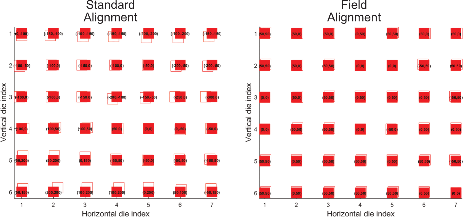
To overcome the limitations caused by using a single, global alignment for a whole wafer, we now have the option to perform local alignment on each die. This new method, as evidenced by the image below, greatly improves alignment precision on each die, reducing both the overall offset and the die-to-die variation. In this demo, standard alignment (left) shows offsets in the ±300 nm range. While all dies are within specification, the offset still varies by up to 500 nm die-to-die. On the other hand, field alignment (right) greatly improves the results, such that all dies exhibit offsets in the ±50 nm range (i.e., the resolution of the verniers used for this test).
Left: Standard (global) alignment. Right: Field alignment. Vertical and horizontal axes indicate the die index and its relative position on the test sample (not to scale). Each die is labeled with its respective (X,Y) offset in nm, with solid squares marking nominal position and red outlines marking the offset position. If the squares overlap at all, this represents "in-spec" alignment.
This improved precision does come at the cost of longer exposure times, however, since the system now has to scan and measure alignment marks for each die being patterned. However, this is a reasonable cost to pay when poor alignment is detrimental to device performance. Please note that this new technique is only available for topside alignment—it cannot be used for backside alignment due to the requirements for this procedure.
If you are interested in using this new field alignment feature, a new document detailing the procedure is available by the tool, and in our Knowledge Base. Also, please do not hesitate in submitting a training request via LMACS if you wish to get hands-on training. For more information, please contact Gustavo de Oliveira.
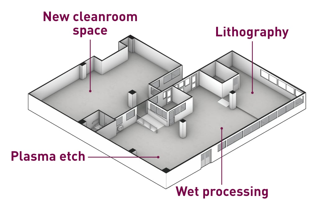
nanoFAB Unveils Cleanroom Expansion
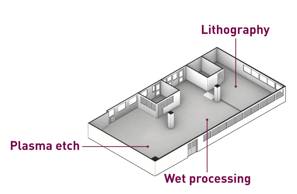
The nanoFAB has completed a large cleanroom expansion, marking a significant milestone in our 25-year history. This expansion represents a strategic investment in supporting the commercial and academic growth of semiconductor manufacturing and materials characterization at the nanoFAB. Through this expansion we are firmly establishing our role as a regional and national contributor to academic and commercial technology developments.
The nanoFAB is an open-access centre specializing in academic research and industry development in micro/nano fabrication and characterization. We provide training and access to over $100M in advanced state-of-the-art equipment and infrastructure to support hundreds of academic and industrial groups across Canada.
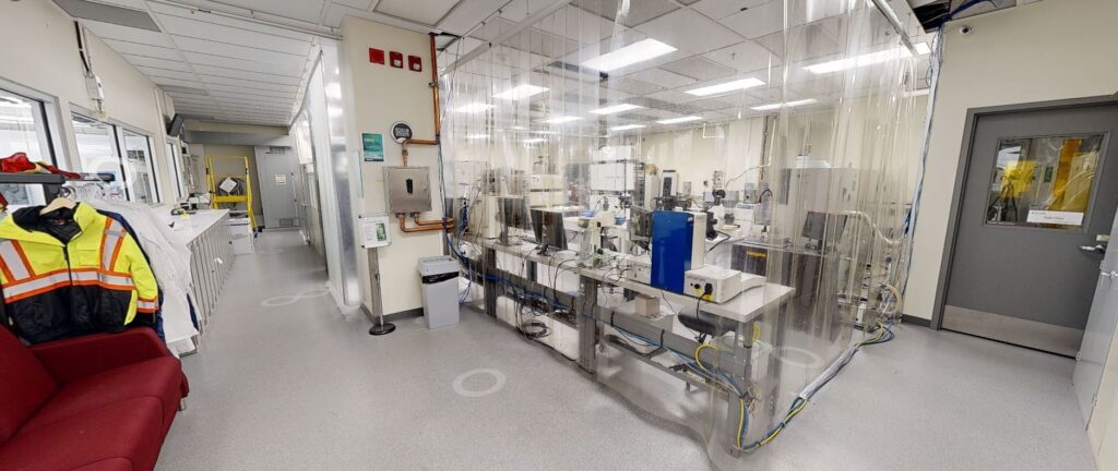
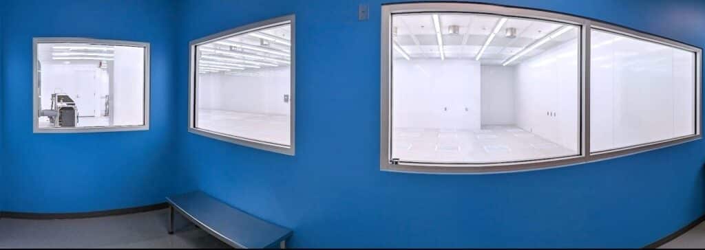
Original nanoFAB lab prior to cleanroom expansionNew nanoFAB cleanroom lab
This critical infrastructure upgrade is set to deliver substantial benefits:
Enhanced Capabilities and Capacity: The expansion directly addresses increased demand for industry hiring and growth, constrained by the lack of space for manufacturing activities. This new cleanroom space will allow for the installation of new equipment, enable hiring of new industrial employees, and create enhanced training opportunities for post-secondary students—boosting productivity, while filling capability gaps that will facilitate industry scale-up and research innovation activities in semiconductor device fabrication.
Driving Economic Diversification: The nanoFAB plays a vital role in fostering economic diversification and entrepreneurship, through providing access state-of-the-art capabilities allowing for technology development. This expansion will further support the development of high-value semiconductor manufacturing, particularly in areas such as energy, advanced electronics, sensing, and quantum systems. It aligns with our goal of strengthening innovation in Alberta and Canada by supporting a critical and growing mass of R&D activities.
Training the Next Generation of Talent: The nanoFAB is a crucial training ground for in-demand talent with hands-on experience in semiconductor manufacturing and materials characterization. This expansion will continue to support the development of highly skilled engineers, scientists, and technicians. The skills developed at the nanoFAB support a growing industry that contributes to economic diversification and the expansion of high-value manufacturing in Canada.
Strengthening Research and Innovation: The expanded cleanroom aligns with our strategic goals of attracting and retaining talent, developing open-access, sustainable infrastructure, and being able to support the growth of research, teaching, and commercialization activities within the University of Alberta. It also supports our broader goals of building a resilient local technology ecosystem that supports the scale-up of innovative hardware manufacturing capabilities.
Our cleanroom expansion, coupled with our ongoing support from industry partners and provincial and federal governments, underscores our strong commitment to being a catalyst for translating laboratory discoveries into high-value commercial outcomes, driving innovation and economic prosperity for Alberta and Canada.
For enquiries regarding this expansion, please contact nanofab@ualberta.ca.
Career Opportunity - Hyperlume Inc.
The nanoFAB is pleased to post the following two Front End Process Engineer career opportunities at Hyperlume.
The details of the positions, including responsibilities, qualifications, experience, and education are listed in the following links:
In semiconductor processing, packaging is a critical step in finishing a final product. After completing the dicing process to singulate dies from a larger substrate, the cut dies generally remain affixed to dicing tape. It can be difficult to manually remove the dies without scratching or rubbing against one another, causing chipping or other damage. A die expander allows for the tape to be stretched on expander rings, separating the dies for easier removal or shipping.
We are happy to announce the addition of a Hugle Model-1810 Die Matrix Expander to the nanoFAB's tool lineup. This expander is capable of accommodating diced specimens up to 150 mm in diameter. It is equipped with a heated chuck, allowing for easier separation of the dies without delamination from the tape, as well as a preheat timer, which helps with process repeatability. The stage expansion distance is adjustable, allowing for customized spacing between the dies. The system also includes an automated cutter tape separation system for ease of use. Previously, without the use of this tool, users in our facility needed to mount diced 150 mm wafers onto the expander ring by hand, a task that often required two people to do!
We hope that the addition of this new system in our toolset will facilitate the final processing and packaging of the many devices fabricated in our open-access facility. Please submit an equipment training request via LMACS if you wish to get trained on the die expander. For more information, please contact Breanna Cherkawski.
Please see below for some videos of the tool in action:
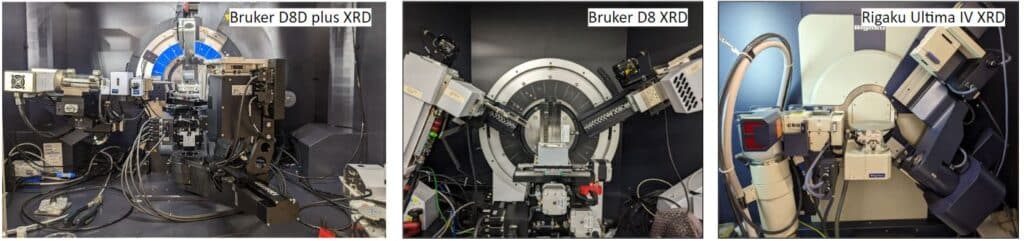
Advanced XRD techniques and applications on Bruker D8D plus diffractometer
The nanoFAB is pleased to announce that advanced In-Plane Diffraction (Non-Coplanar Scan), Pole Figure Measurement, 2D Stress Measurement, and Multi-Angle Scattering (SAXS/WAXS) are fully commissioned on the Bruker D8 DISCOVER Plus X-Ray Diffractometer .
IN-PLANE DIFFRACTION (NON-COPLANAR SCAN): With standard diffraction geometries (coplanar scan), such as the Bragg-Brentano geometry, X-rays penetrate to a certain depth into the sample, and the diffraction from lattice planes parallel to the sample surface is measured. In case of ultra-thin films, X-rays completely transmit and no diffraction is observed from the thin film with the standard coplanar scan. In these circumstances, in-plane diffraction enabled by non-coplanar scan provides effective and efficient analysis, in which both the incident and diffracted beams are nearly parallel to the sample surface, as the detector scans in the plane of the horizontally positioned sample. In-plane diffraction has two major features:
(1) The penetration depth of the X-ray is limited to the top surface of the sample. By setting the X-ray incidence at the critical angle or slightly higher, ultra–thin films and the texture of surface layers can be analyzed.
(2) The technique measures lattice planes that are (nearly) perpendicular to the sample surface, which are inaccessible by other techniques. This second feature is a key difference between the in-plane grazing incidence diffraction (IP-GID) vs. the conventional GID with coplanar scan. Figure 1 shows the setup of in-plane diffraction (non-coplanar scan) on the Bruker D8D plus XRD, as compared to coplanar symmetric 2theta/theta scan for powder diffraction on the Bruker D8 XRD and coplanar GID for thin-film applications on the Rigaku XRD.
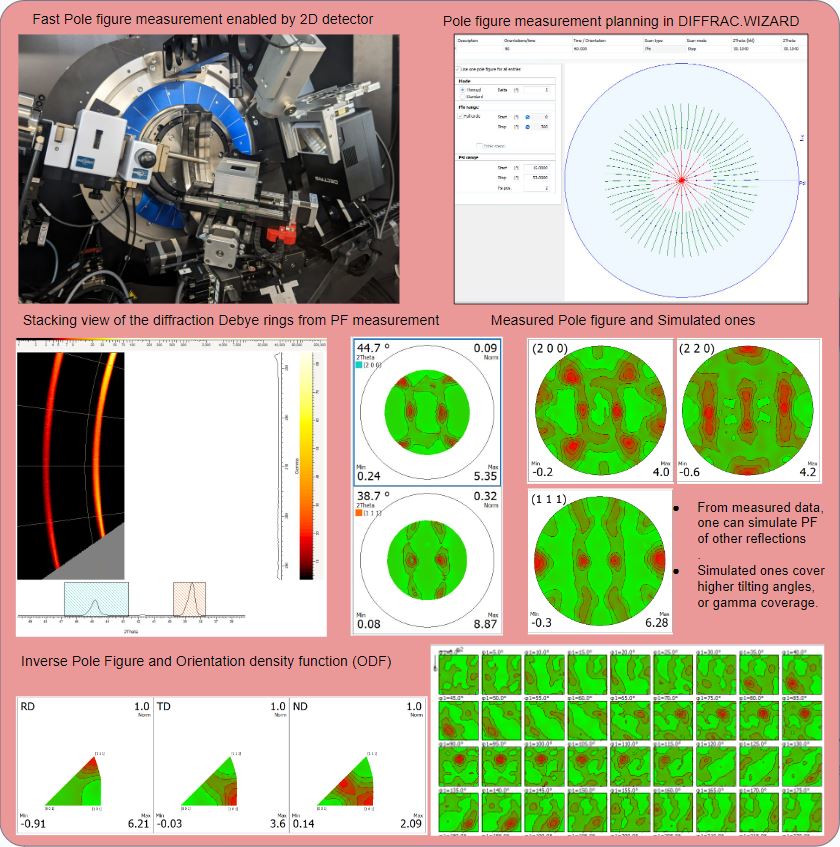
QUANTITATIVE TEXTURE ANALYSIS: The presence of crystallographic texture (preferred orientation) in polycrystalline materials has a significant effect on the anisotropy of the materials properties. Therefore, it is critically important to obtain a qualitative/quantitative description of the orientation distribution of crystallites, or the orientation distribution function (ODF) in order to characterize and predict their properties. While direct measurement of the ODF is very challenging, pole figures (PF) can be measured to reconstruct the ODF experimentally, where the diffraction angle is fixed and the diffracted intensity of a certain lattice plane is record by varying two geometrical parameters, such as the alpha angle (tilt angle of the scattering vector from the surface normal direction of a sample) and the beta angle (rotation angle of the scattering vector around the surface normal direction of a sample). The sensitive and large size 2D detector available on the Bruker D8D plus provides large coverage in Gamma and 2Theta, thus high speed and high throughput PF measurement (compared to measurement using a 0D or 1D detector), by taking 2D frames as continuous scans in PHI (the azimuthal angle) at successive values of Psi (the tilt angle).
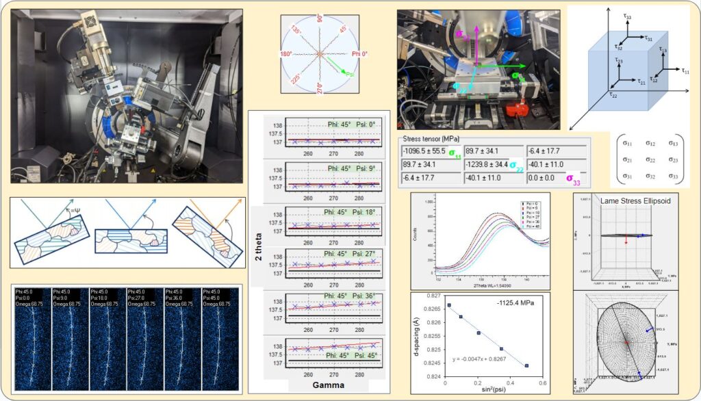
RESIDUAL STRESS ANALYSIS: Residual stress, created during the materials manufacturing process or accumulated during operation, can have serious negative effects on a product's quality, performance, and durability, as it may result in cracks and delamination of the films, as well as deformation of the substrate depending on the adhesion strength between the film and the substrate. Residual stress X-ray diffraction is one of the techniques for evaluating the near-surface residual stress with high accuracy, which is non-destructive and is applicable to polycrystalline materials with moderate to fine grain sizes. In X-ray diffraction residual stress measurement, the strain in the crystal lattice is measured using the changes in the d-spacing of the crystal lattice planes as the strain gauge, and the residual stress producing the strain is calculated assuming a linear elastic distortion of the crystal lattice. The most commonly used method for XRD stress determination is the sin2(Psi) method. By measuring the change in the d-spacing of a suitable lattice plane for at least two different tilting angles (Psi), the stress present in the plane of sample surface can be calculated from the slope of the d vs. sin2(Psi) plot. Our Bruker D8D plus XRD provides 2D stress measurement with the side inclination method, enabled by Psi tilt and PHI rotation of the Eulerian cradle, together with the large Gamma coverage of the 2D detector. 2D stress analysis measures not only the peak position but also the shape of the diffraction Debye rings. Essentially, it describes the curvature of the diffraction rings as the scattering vector tilted away from the surface normal, providing a more generalization solution than the simple sin2(Psi) peak position analysis, which is a special condition of the 2D stress analysis. The procedure of 2D stress measurement is similar to that of 2D pole figure measurement, except that a higher-angle diffraction peak needs to be used.
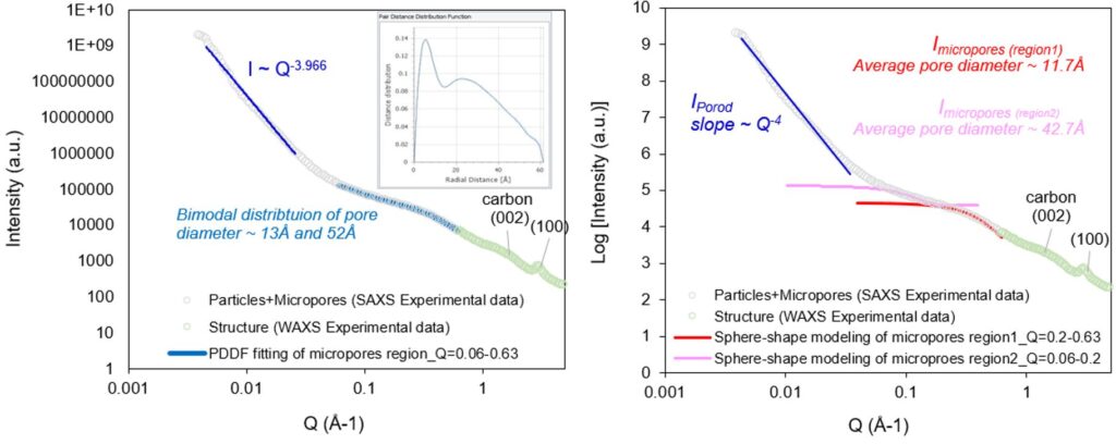
MULTI-ANGLE SCATTERING (SAXS/WAXS) ANALYSIS: Small-Angle X-ray Scattering (SAXS) analyzes the elastic scattering behavior of X-rays when traveling through the material, recording their scattering at small angles (typically 0.1 - 10°). SAXS quantifies nano-scale density differences in a sample, enabling characterization of particle sizes, shapes, distribution, pore sizes, characteristic distances of partially ordered materials, and much more. Wide-Angle X-ray Scattering (WAXS) is similar to SAXS, except that the distance from sample to the detector is shorter and thus diffraction maxima at larger angles are observed. WAXS usually covers 2theta 5-60 degree, revealing scattering/diffraction at sub-nanometer scale such as crystalline lattice planes. Multi-angle scattering analysis utilizes both SAXS and WAXS in conjunction to probe a wide range of length scale from an angstrom to a micrometer, revealing a full picture of the materials structure.
In-plane diffraction, pole figure, and 2D stress measurements are now available for user training and staff analysis. Please see the application examples and discussions below for more details. If you are interested in utilizing these techniques for your materials characterization, please submit a training request on LMACS. If you have any questions, please feel free to contact Dr. Xuehai Tan (xtan@ualberta.ca) and Peng Li (peng.Li@ualberta.ca) – the Characterization Group Manager.
Figure 1 - Comparison of non-coplanar scan, coplanar symmetric scan, and coplanar GID scan setups on nanoFAB XRD systems.
Application Examples
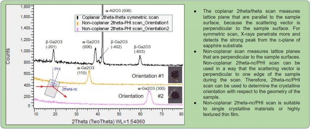
Sample: Epitaxially grown Ga2O3 thin film on sapphire substrate Analysis: In-plane diffraction (Non-coplanar scan) Application: Coupling non-coplanar 2theta-nc / PHI scan and coplanar 2theta/theta symmetric scan to characterize epitaxially grown Ga2O3 thin film on sapphire substrate.
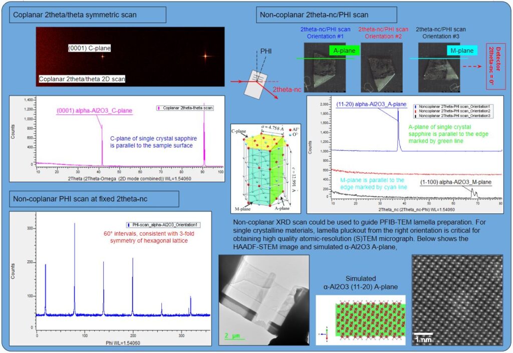
Sample: Single crystal sapphire α-Al2O3 Analysis: In-plane diffraction (Non-coplanar scan) Application: Coupling different non-coplanar scans and coplanar symmetric scan to characterize single crystalline materials. An example is given on how in-plane diffraction could be used to guide PFIB-TEM lamella preparation.
Sample: Soda can Al sheet produced through cold-rolling Analysis: Fast pole figure measurement enabled by 2D detector Application: Texture analysis of the orientation distribution of crystallites from pole figure measurements.
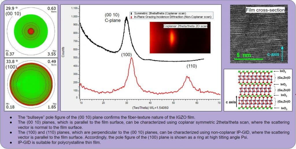
Sample: Fiber-textured In-Ga-Zn-O (CAAC-IGZO) film on Si substrate for 3D glasses-free holographic displays Analysis: Pole figure, coplanar symmetric scan, non-coplanar in-plane GID, PIB-STEM Application: A correlative study of fiber-textured IGZO film using pole figure, coplanar and non-coplanar XRD (In-plane GID), and PFIB-STEM microscopy of the film cross section. Sample Courtesy:Avalon Holographics Inc., Edmonton
Sample: Fe film with compressive stress Analysis: 2D stress analysis Application: A more generalization residual stress analysis solution than the simple sin2(Psi) peak position analysis
Sample: A hard carbon with rich closed pores. Analysis: Multi-angle X-ray scattering Application: Coupling SAXS and WAXS to investigate the internal pore sizes and the short-range ordered carbon structure.
Optical Emission Interferometry (OEI) in the Plasma-Therm Versaline PECVD
Overview
In plasma-enhanced chemical vapour deposition (PECVD) tools, the deposition rate of deposited films can often fluctuate with relative gas concentrations, material build-up on the chamber walls, and other mechanisms that make timed depositions inconsistent. To combat this problem, a simple technique called Optical Emission Interferometry (OEI) can be used. OEI provides a more robust form of deposition control based on the interference of light reflected off of the growing film to precisely hit target film thicknesses.
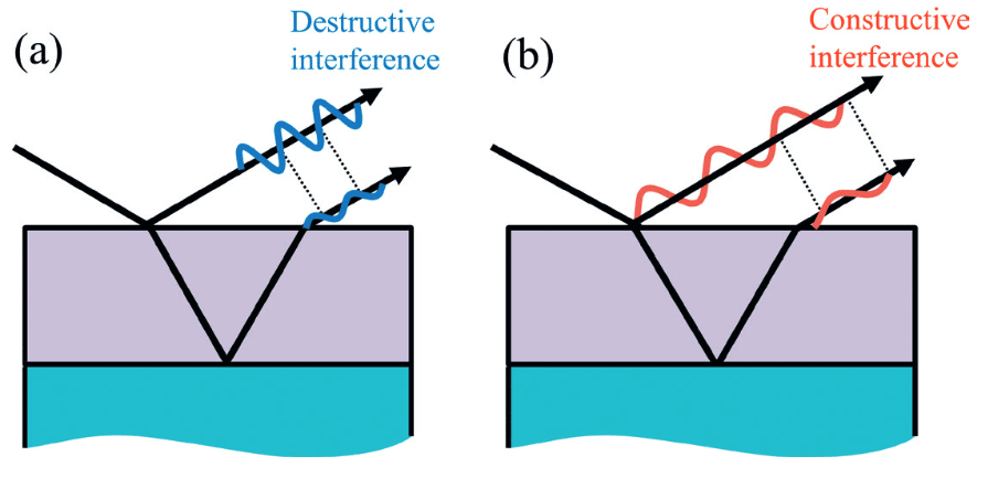
OEI uses similar principles to other interferometric tools like the Filmetrics F50-UV; the intensity of light at a single wavelength reflected off of a thin film will vary depending on the wavelength of light and the optical thickness of the film. This is due to the relative phase difference between light reflected off the top surface of the film and at the film-substrate interface, i.e., conditions of constructive and destructive interference (shown in Fig. 1). Across a broad spectrum of wavelengths, this can be used to fit to both refractive index and film thickness robustly (as Filmetrics does). However, if the intensity of light reflected off of a growing film is recorded continuously, the intensity at a "single" wavelength will oscillate approximately sinusoidally as the thickness increases (satisfying constructive and destructive interference conditions at specific thicknesses)—this is the fundamental premise of OEI. By noting when the extrema occur during film growth, the period of this oscillation (T) can be used to measure the deposition rate of the film, since T is set by the phase conditions for constructive/destructive interference. T = λ/(2n); where λ is the wavelength of interest and n is the refractive index of the material at this wavelength.
Figure 1. Phase conditions for destructive and constructive interference of light reflected off of a thin film, from H. G. Tompkins, and J. N. Hilfiker, Spectroscopic Ellipsometry: Practical Application to Thin Film Characterization (Momentum Press, 2016).
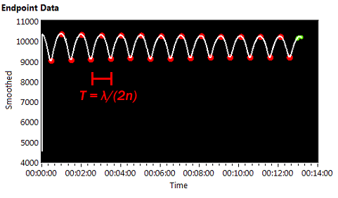
To use OEI in the Plasma-Therm Versaline PECVD, light produced by the plasma is reflected off of the growing film and collected by a spectrometer centred above the wafer for plasma monitoring. The Plasma-Therm EndpointWorks software package is then used to monitor the evolution in time of the spectral intensity emitted from the plasma within a narrow range of wavelengths. Choosing a range that encompasses an emission line of a typical gas/radical species within the plasma produces the oscillatory data shown in Fig. 2. Values of T are calculated based on known values of n and λ to give an estimate of the deposition rate based on the spacing of the extrema. Thus, in order to function correctly, each OEI recipe requires the user to have knowledge of both the growing film (single wavelength refractive index) and of typical optical emission lines (usable wavelengths) within the plasma.
Figure 2. EndpointWorks Thickness Detector data for a growing SiO2 film.
Wavelength choice
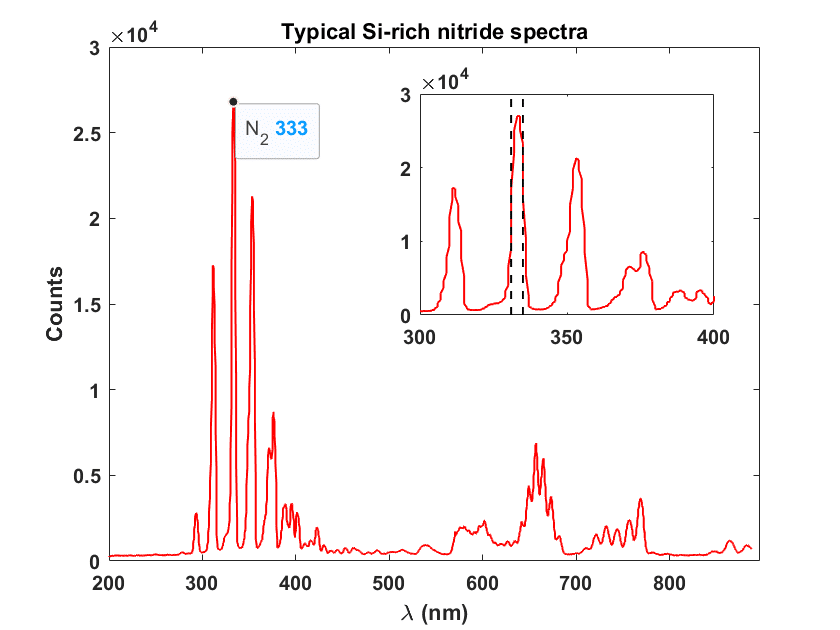
The choice of what wavelength to use for OEI depends on the chemistry of the plasma in question, since each gas/radical species emits light at different wavelengths (depending on its electronic transitions), and thus the available wavelengths will differ for each recipe. Potential emission lines are further limited if the gas species characteristic of an emission line is consumed during the reaction. The intensity of these reactant emission lines will fluctuate as the film grows and as the local gas concentration changes. In contrast, the intensity of an emission line of an inert gas (He, Ar, or N2 are often used to dilute the reactants) will be much more stable, and will provide a reduction in noise in the reflected light. This leads to a more clearly defined periodic signal, where the extrema can be easily identified in software. Additionally, since variation in T is linear with the wavelength of light used, the choice of shorter wavelengths will reduce the period of oscillation, lending the OEI method more sensitivity and flexibility to accurately measure thinner films. Note, for films that are optically absorbing (e.g. a-Si and Si-rich nitrides), the film will absorb more strongly at shorter wavelengths, decreasing the amplitude of the oscillation as the film grows. Ultimately, this decay reaches a point where extrema cannot be identified past a certain thickness. A general rule of thumb is to choose the shortest wavelength inert gas emission line that is not strongly absorbed by the depositing film. A typical spectrum collected during deposition is shown in Fig. 3, where a N2 emission line at ~333 nm is highlighted, being suitable for the gas chemistry involved. For more details on choosing an emission line appropriate for your deposition, please see the Plasma-Therm Versaline PECVD OEI recipe development How-To on the nanoFAB's Confluence Knowledge Base.
Figure 3. Typical plasma emission spectrum (as measured on the Versaline's integrated Ocean Optics spectrometer) for the deposition of Si-rich nitride. Inset: full-width at half-max (dashed lines) of the N2 emission line centred at ~333 nm.
OEI controlled deposition recipes are currently qualified for SiO2 Dep ("OEI SiO2 Dep") and Stoichiometric Nitride ("OEI Stoichiometric Nitride") recipes, with an OEI recipe in progress for the Si-Rich Nitride. For user-developed films that differ from these established recipes, users are welcome to qualify their own OEI recipes following the Step-by-step instructions in the linked OEI recipe development How-To. If you encounter problems setting up your OEI recipe on EndpointWorks, please contact Tim Harrison (tr1@ualberta.ca).