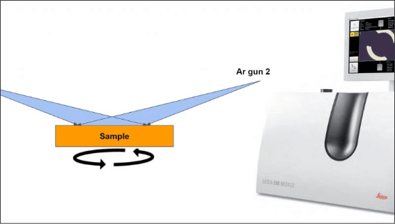
RES102 BIB Ion Milling System equipped with two Ar guns
Among general electron microscopy applications, Electron Backscatter Diffraction (EBSD) is a surface technique – typical probing depth is in the range of a few tens nm for a beam energy of 20 kV. Smooth and damage-free surface is critically important to obtain high quality EBSD data. Compared to conventional mechanical polishing techniques, which can result in very rough surfaces and a thick damaged layer, low energy beam at grazing incident angle and rotating stage on the RES102 can effectively polish the surface to reduce roughness and remove the damaged layer.
With the programmable recipes of flexible parameters (beam energy, beam current, incident angle, stage rotating speed), the RES102 BIB has produced very nice results for our users for EBSD analysis. See recent examples below.
Application Examples (EBSD)
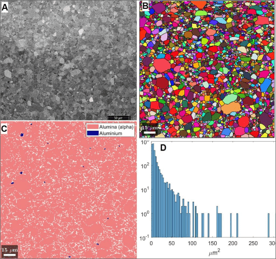
Sample: 3D printed Alumina for structural applications
Sample Courtesy: Cass (Haoyang) Li, Dr. James Hogan, Mechanical Engineering Department, Faculty of Engineering, University of Alberta
Ion Milling process:
8 kV, 3 mA, 3.5 degrees, 1.5 rmp for 120 mins
8 kV, 2 mA, 2.5 degrees, 1.5 rmp for 60 mins
EBSD mapping: 175 µm x 175 µm, stepsize 50 nm
(A) SEM image; (B) Orientation map; (C) Phase maps of Alumina and Aluminium; (D) Grain size distribution
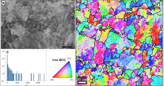
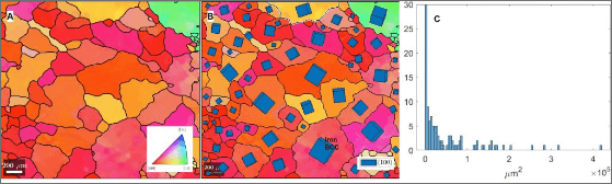
Sample: Rail Steel
Sample Courtesy: Stephen Okocha, Drs. Ben Jar and Michael Hendry, Mechanical Engineering Department, Civil and Environmental Engineering Department, Faculty of Engineering, University of Alberta
Ion Milling process:
8 kV, 3 mA, 2.5 degrees, 1.5 rmp for 60 mins
6 kV, 2 mA, 2.5 degrees, 1.5 rmp for 60 mins
EBSD mapping: 300 µm x 300 µm, stepsize 250 nm
(A) SEM image; (B) Orientation map; (C) Grain size distribution
Sample: Al-Cr-Fe-Ni medium-entropy alloy (MEA)
Sample Courtesy: Guijiang Diao, Dr. Dongyang Li, Chemical and Materials Engineering Department, Faculty of Engineering, University of Alberta
Ion Milling process:
8 kV, 3 mA, 3.5 degrees, 1.5 rmp for 60 mins
5 kV, 2 mA, 2.5 degrees, 1.5 rmp for 60 mins
EBSD mapping: 2500 µm x 1500 µm, stepsize 500 nm
(A) Orientation map; (B) Crystal unit cell orientation and (C) Grain Size Distribution
The RES102 ion milling system is now available to general users for both staff analysis and user training. Any users interested in getting trained on this tool or staff analysis should submit a request on LMACS. If you have any questions, please contact the tool managers Drs. Nas Yousefi and Shihong Xu or Peng Li – the Characterization Group Manager
In-situ heating S/TEM is available
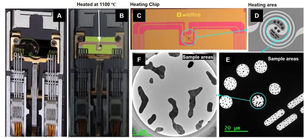
The nanoFAB is pleased to announce that the DENS solutions In-Situ Lightning TEM holder is fully commissioned and in-situ heating TEM analysis is available on the JEOL JEM-ARM200CF S/TEM Microscope.
The DENS lightning in-situ heating platform utilizes the state-of-the-art MEMS technology to create the lab-on-chip environment that replicates the real-life heating conditions inside the TEM, which provides unprecedented control and accuracy over temperature:
8 contacts for simultaneous heating and biasing analysis
Double tilted holder
Maximum heating temperature of 1100 °C
Flexible and customizable heating profiles
Compatible with EDX analysis
All these unique features enable dynamic analysis of morphological (imaging), structural (diffraction) and compositional (EDX) changes of materials at very high spatial resolution on the JEOL ARM S/TEM.
The in-situ heating TEM analysis is now available to all users. If you have needs for these analysis, please submit a sample analysis request with sample details on LMACS. If you have any questions, please feel free to contact Dr. Xuehai Tan (xtan@ualberta.ca) – the primary TEM staff member or Peng Li (Peng.Li@ualberta.ca) – the Characterization Group Manager.
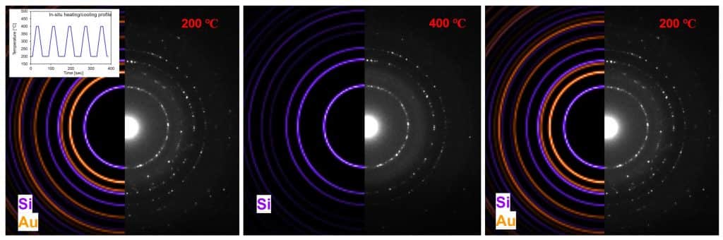
Images show (A) double tilted Dens Lightning holder, (B) heating chip being heated at 1100°C, (C) (D) heating chip and (E) (F) sample areas on the chip.
Application Examples
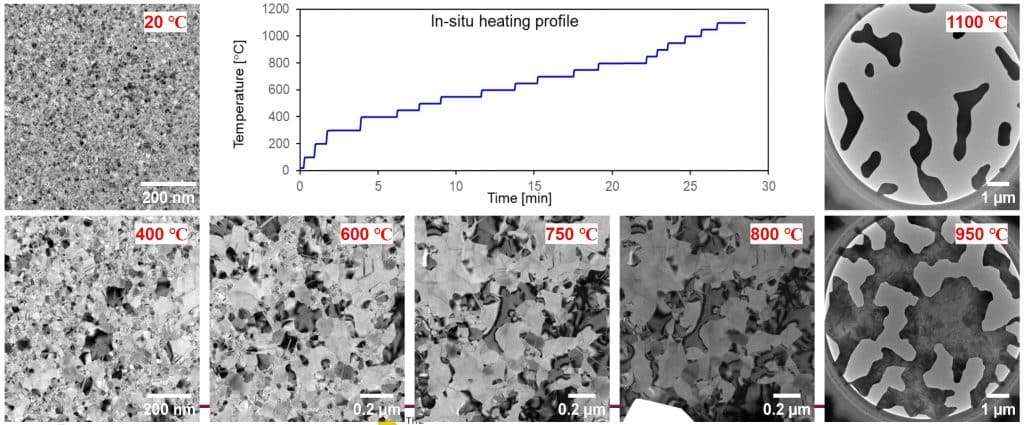
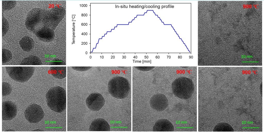
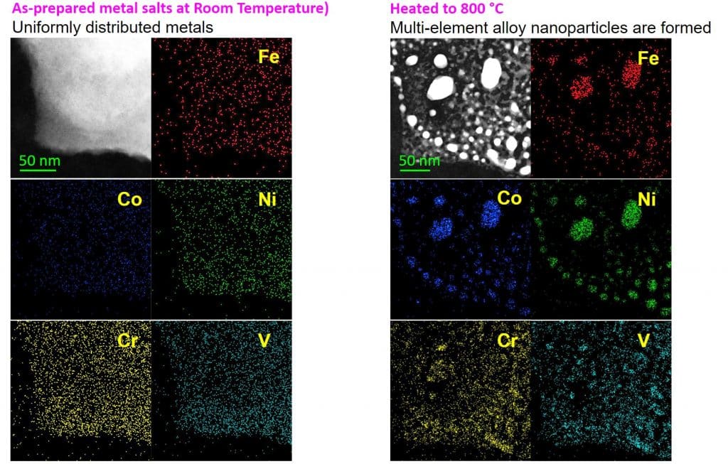
Recrystallization and melting of polycrystalline Au film heated up to 1100 °CMorphological analysis by DF-STEM images: formation of particles up to 800 °CCompositional analysis by EDX: confirming the composition of the particles. Despite the influence of infrared radiation emitted from the heating device, EDS elemental mapping is acquired at elevated temperature (800 °C) during the in-situ heating.
Kurt J. Lesker 150LX ALD system now open for training
The nanoFAB is pleased to announce that our newly installed and commissioned KJLC 150LX Atomic Layer Deposition system is now fully operational and available for training to all nanoFAB users. The ALD offers excellent uniformity and controlled growth of a variety of films on an atomic scale. Its high-vacuum load-lock and UHV-type sealing, combined with near-constant high-purity Ar flow, enable high-purity process conditions and excellent quality films.
Main system features include:
Single wafer transfer load-lock
Substrate heating up to 500 °C
150 mm platen, with an available carrier for samples <150 mm
Thermal and plasma-enhanced (PE-ALD) processes available
In situ film growth monitoring using Film Sense FS-1EX multiwavelength ellipsometer
The KJLC 150LX ALD is available to users for self-use (after training) and fee-for-service work. Any users interested in getting trained on this tool should submit a training request via LMACS. If you have any questions, please contact Aaron Hryciw (ahryciw@ualberta.ca) or Scott Munro (smunro@ualberta.ca).
nGauge AFM is now Available at nanoFAB
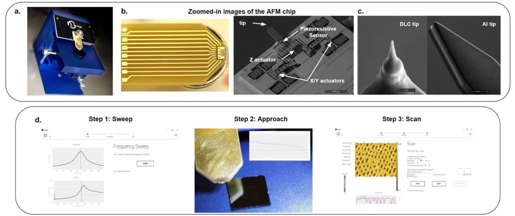
The nanoFAB is pleased to announce that the new Atomic Force Microscopy system, the ICSPI nGauge AFM, has been successfully installed and is operational now. This benchtop AFM allows nanoscale topography data collection with 3 easy steps: automatic sweep, approach, and scan. The nGauge AFM is a laserless system, based on a patented AFM-on-a-chip technology. In this new technology, all of the sensors and scanners of a traditional AFM have been integrated onto a single chip, so you can capture routine scans in just over a minute.
The nGauge AFM operates in the tapping mode and generates topography, phase, and error images simultaneously for any solid samples (including conductive and non-conductive, but not liquid samples). nGauge AFM tips are made of durable materials like diamond-like carbon (DLC) and aluminum oxide, which are also integrated onto the AFM chip, enabling hundreds (or thousands) of scans possible with each tip.
(a) The benchtop nGauge AFM. (b) AFM chip and its integrated components. (c) Front view of the Diamond-Like Carbon and Aluminum tips. (d) 3-step scan collection via nGauge AFM
nGauge AFM Specifications:
Max scan area: 20 x 20 μm
Z Range: 10 μm
Scan speed: 80 seconds (256 x 256 pixel, 20 x 20 μm)
Max scan resolution: 1024 x 1024 pixels (5 minutes)
Noise floor: <0.5 nm rms
XY Scanner resolution: <0.5 nm
Images: Topography, Phase, Error
Approach: Automatic
Max sample size: 100 mm x 50 mm x 16 mm
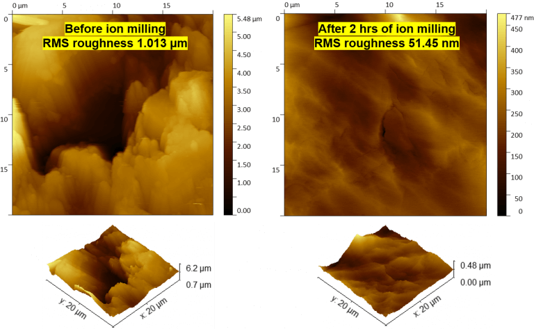
Sample: Shale (before and after ion milling processes) Sample courtesy of Graham Spray, M.Sc., P.Geo., AGAT Laboratorie.
Diamond-Like Carbon (DLC) Tip Specification:
nGauge AFM tips are made of diamond-like carbon materials with high aspect ratio offering excellent lateral resolution and excellent contamination resistance.
Tip radius: <20 nm
Tip height: >1 μm
Cone angle: <10°
Aspect ratio: >3
Tilt compensation: 15°
Tip post height: 3 μm
Tip shape: Conical
Tip material: Diamond-like carbon\
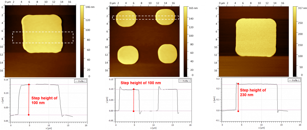
Sample: Patterned Cr + Au / Ti on Si chip
Cantilever Specifications:
nGauge AFM tips are located at the very end of the cantilever beam and are integrated onto a micro-electro-mechanical systems (MEMS) chip. The chip features integrated lateral and vertical actuators and piezoresistive sensors.
Shape: Beam
Length: 30 μm
Width: 6 μm
Thickness: 3 μm
Resonant Frequency: 8 kHz (typical: 7.3–8.7 kHz)
Stiffness: 0.1 N/m
The nGauge AFM is now available to users for both staff analysis and self-use/user training provided they purchase own nGauge AFM chip. Any users interested in getting trained on this tool or staff analysis should submit a request via LMACS. If you have any questions, please contact Dr. Nas Yousefi or Peng Li – the Characterization Group Manager.
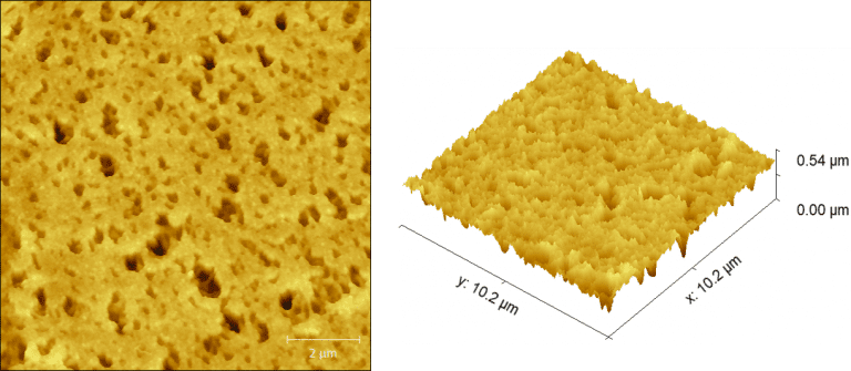
Sample: Polymeric Membrane Sample courtesy of Dr. Sadrzadeh, Mechanical Engineering Department, Faculty of Engineering, University of Alberta.