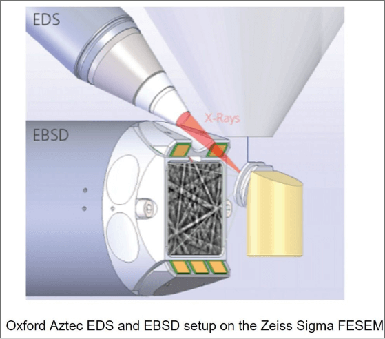
Electron & Ion Microscopy (SEM, FIB and TEM) provides morphological and compositional analysis with ultra high spatial resolution but lack of larger macroscopic context. It is also challenging to obtain analysis and observations with multiple sources from identical locations of the same devices/samples, in order to obtain comprehensive data.
Software solutions are now installed and commissioned in the following microscopes, providing large area imaging and correlative workflow:
ATLAS on Zeiss Sigma FESEM ATLAS on Zeiss EVO SEM MAPS on ThermoFisher Hydra Plasma FIB/SEM
These software packages enable automatic workflow of multi-scale (from cm to nm), multi-platform (optical, x-ray, electron and ion microscopy and spectroscopy) and multi-dimensional (2D, 3D and 4D) characterization. Please see the application examples below of how the workflow can provide correlative analysis by linking Optical, Raman, AFM, XRM, SEM, FIB, and TEM data.
ATLAS and MAPS software are now available for user training. If you are interested in utilizing the workflow for your material characterization, please submit a training request on LMACS. If you have any questions, please feel free to contact Shihong Xu (shihongx@ualberta.ca), Josh Perkin (jperkins@ualberta.ca) or Peng Li (peng.li@ualberta.ca).
Application Examples
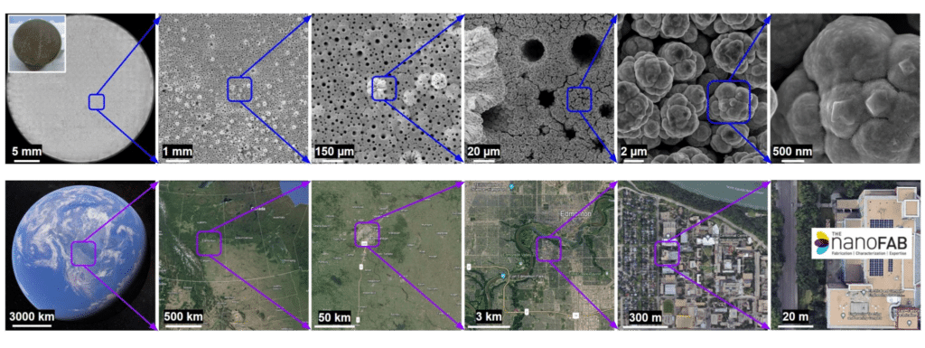
Sample: Porous Ni film Application: Large area imaging for multi-scale analysis (Google Earth like images with high spatial resolution) Instrument: Zeiss Sigma FESEM
A series of images seamlessly integrates correlative imaging to showcase a progressively zoomed view from a large object to a microscopic structure, transitioning from a satellite view of Earth to the intricate details of building layouts.
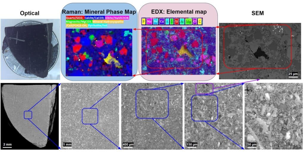
Sample: Shale Application: Multi-scale and correlative SEM/EDX/Raman analysis of elemental and mineral distribution Instruments: Zeiss EVO SEM with Oxford EDX Renishaw inVia Confocal Raman
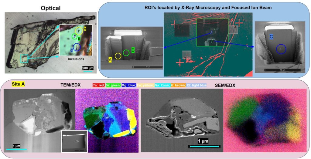
Sample: Mineral inclusions Application: Multi-scale and correlative SEM/EDX/XRM/TEM analysis of mineral inclusions in magnetite-apatite deposits This work is published in Geology (2024) 52 (6): 417–422
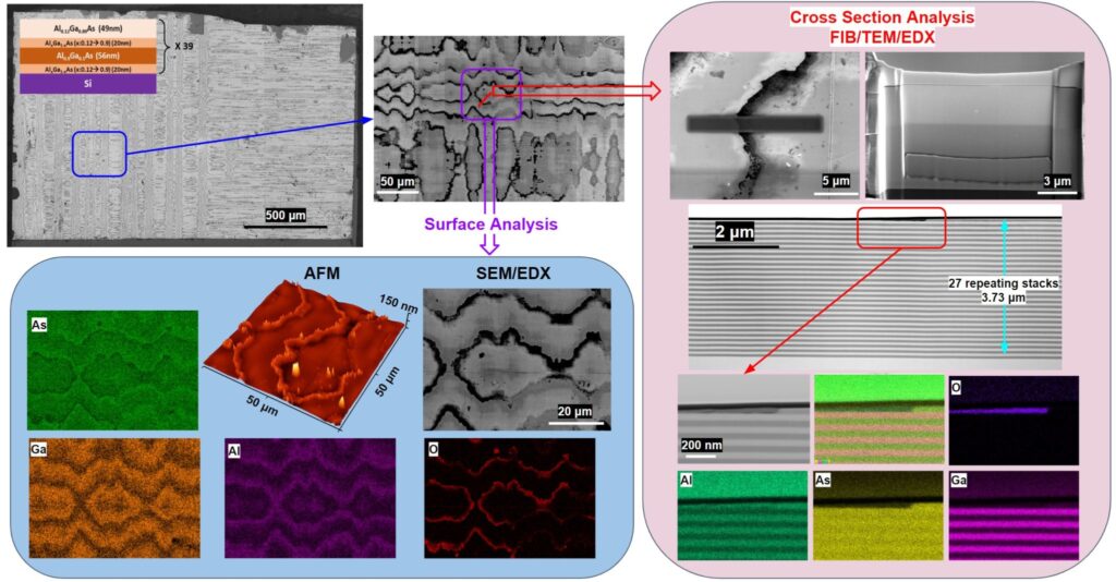
Sample: Multi-layer AlGaAs thin film Application: Correlative SEM/EDX/AFM/TEM analysis to characterize both surface and cross section morphology and composition Instruments: ThermoFisher Hydra Plasma FIB/SEM Bruker Dimension Edge AFM JEOL ARM S/TEM
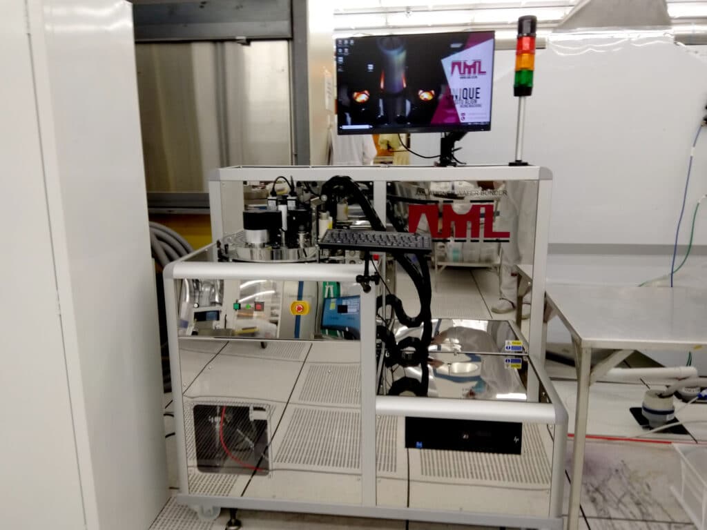
AML Wafer Bonder now available for training
The nanoFAB is pleased to announce an upgrade to our wafer bonding and packaging area, with the recent installation of a wafer bonder from Applied Microengineering Ltd (AML). The AWB-04 wafer aligner-bonder from AML offers a wide range of bonding techniques and process flexibility. Of particular note is its in situ alignment capability, allowing users to verify correct alignment as the wafers are being brought into contact.
Bonding techniques include:
Anodic (borosilicate glass to Si)
Direct (Si to Si)
Eutectic (Si to Si or Si to glass with intermediate metal layer)
Thermocompression (bonding between metal films deposited on both substrates)
Other custom bonding techniques
Technical features:
Up to 150 mm wafer sizes (100 mm and 150 mm hardware available)
In situ alignment (visible and IR) with 1 µm accuracy; manual and automatic (image recognition) alignment procedures available
High vacuum (10-6 Torr)
Wafer separation of 30 mm
Independent platen temperature control, up to 560 °C
Radical activation (RAD) for in situ surface cleaning and activation
Bonding forces up to 40 kN
Anodic bonding voltages up to 2.5 kV, current limits up to 8 mA
Triple-stack anodic bonding
Wafer edge clamping (no contact on bonding surfaces)
Application Examples
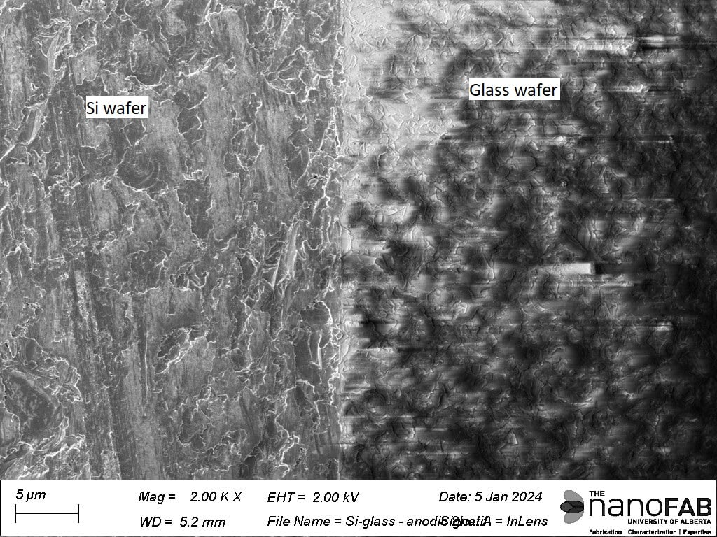
Anodic Bond: borosilicate glass to Si
Cross-sectional SEM (left) and TEM (right) images of bonding interface.
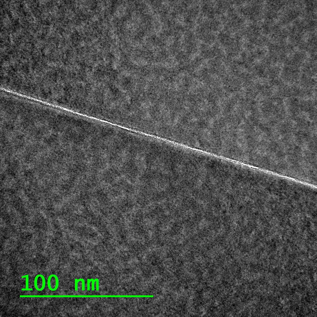
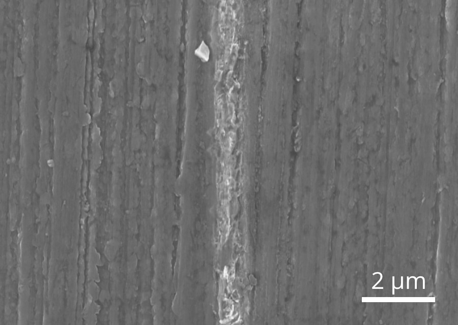
Si–Si Direct Bond: in situ RAD + low-temperature anneal
TEM images of the bonding interfaces of silicon wafers after a low-temperature (250 °C) anneal performed in the AWB-04 chamber without breaking vacuum. The thin amorphous native SiO2 layer can be seen along the interface.
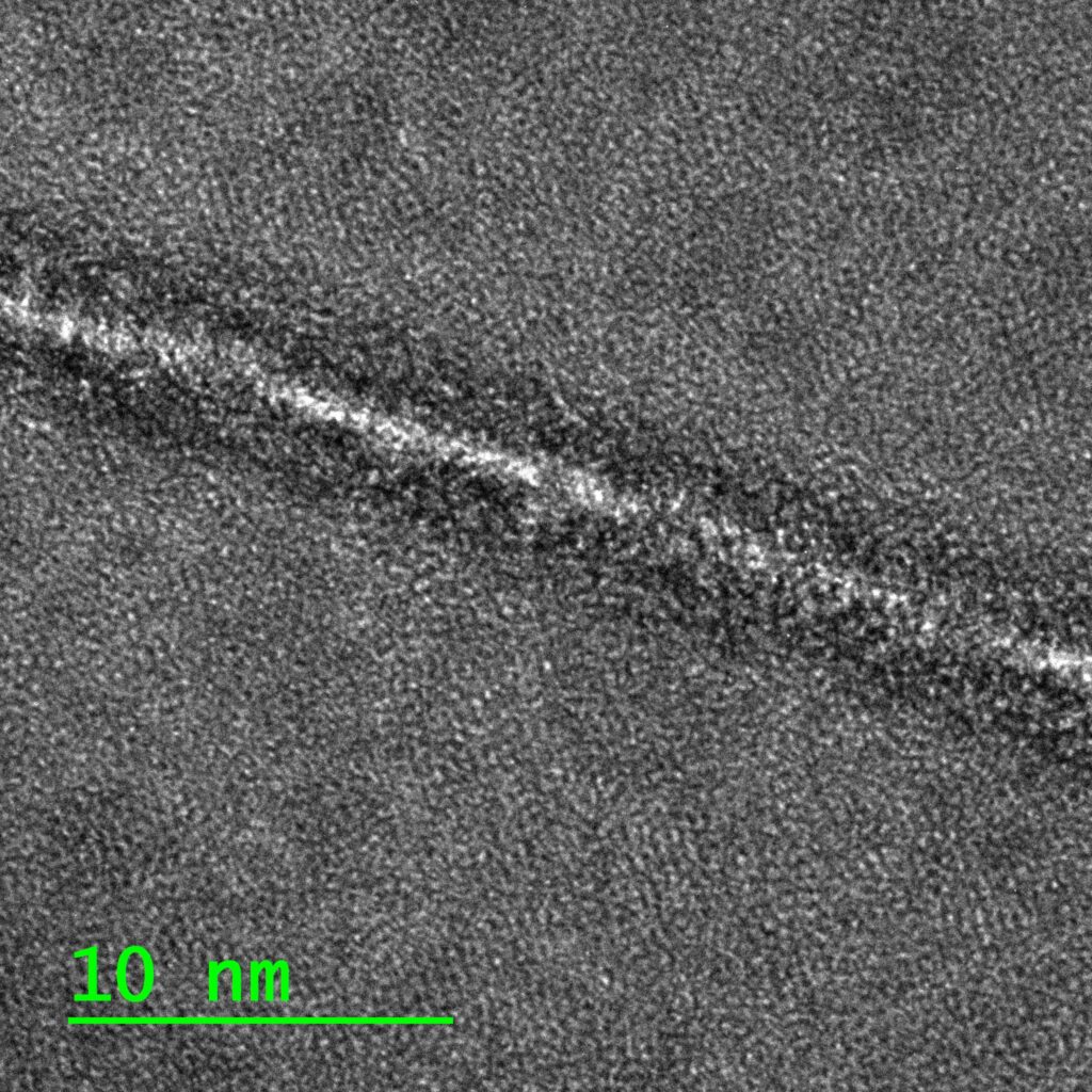
Si–Si Direct Bond: in situ RAD + external high-temperature anneal
TEM images of the bonding interfaces of silicon wafers after a high-temperature (1100 °C) anneal performed in Tystar General Anneal (Tube 6). The thin amorphous native SiO2 layer can be seen along the interface, but has diffused into the bulk Si layer.
Au–Au Thermocompression Bond: Si to Si with Au interlayers
SEM images of silicon wafers bonded via Au–Au thermocompression bonding: full wafer cross-section (left) and close-up of bond interface (right). Patterned Au films are deposited on Si wafers and bonded using moderate temperatures (~300 °C) and high pressures (~7.5 MPa). Images courtesy of Jones Microwave Inc. and RM3.
If you are interested in using the AML wafer bonder in your work, please submit a request through LMACS to receive training. If you have any questions, please feel free to contact Scott Munro or Aaron Hryciw.
New Spray Coating Tool Available
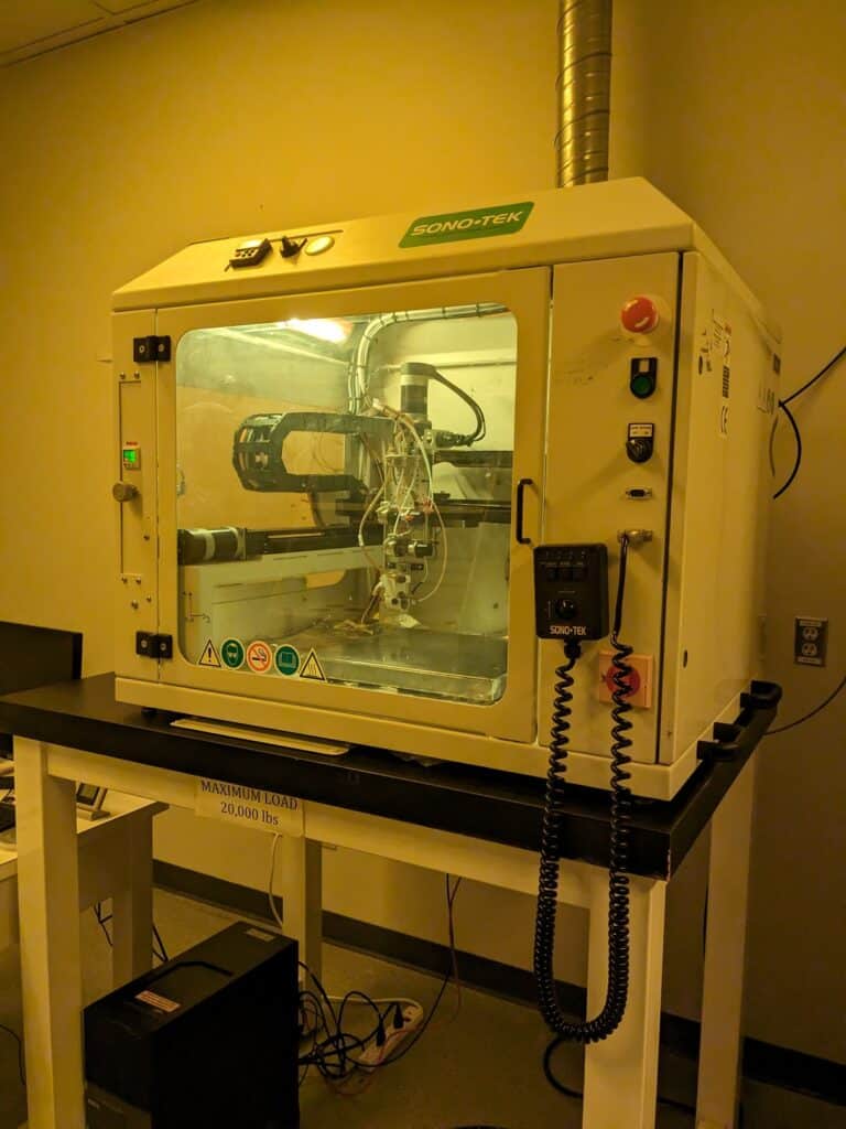
We are happy to announce a new addition to our fabrication tool lineup: a Sono-Tek ExactaCoat Spray Coater. This tool is located in our recently renovated 10k Lithography area (ECERF W1-031); please stay tuned over the coming months as we add more photolithography capabilities to this labspace.
The ExactaCoat, an ultrasonic spray coating system, can accommodate specimens up to 300 mm in diameter. This tool is primarily used for photoresist coating in situations where conventional spin coating is impractical or yields poor results: specimens that are too fragile, exhibit large topographical variations, or possess irregular shapes.
The spray coater offers a particular advantage for specimens where topography presents a challenge to achieving good film uniformity during spin coating: examples include MEMS or microfluidic devices with deep (tens to hundreds of µm) features etched via DRIE or KOH/TMAH. Process development is currently underway to formulate recipes suitable for coating deep and/or high aspect ratio topography wafers. Additionally, spray coating is a valuable technique for those looking to apply photoresist as a dicing protect layer on extremely fragile or through-etched substrates that are not compatible with spin coating.
Sono-Tek ExactaCoat Spray Coater
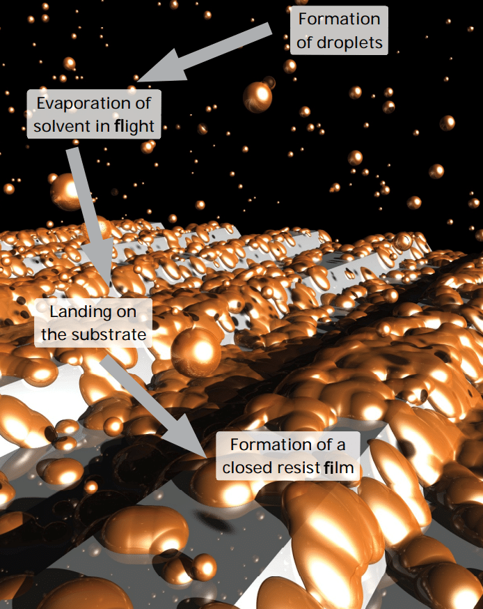
Schematics of the spray coating process (MicroChemicals)
The spray coating process uses high-frequency (ultrasonic) mechanical vibration that is transferred to the liquid in the nozzle. The standing waves created in the liquid are broken up as the liquid exits the nozzle—this aerosolised liquid is then dispensed onto the surface of the specimen as a fine mist.
To coat an extended specimen such as a wafer, the spray of atomised resist is rastered across the work area in overlapping stripes. This is illustrated in the following videos, where a cleanroom wipe is used to show the sprayed resist more clearly.
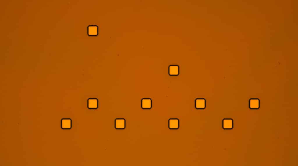
After spray coating a wafer with resist and softbaking, it may be exposed and developed to complete a photolithography process. The following optical microscope images illustrate some preliminary results of photolithography on Si wafers, showcasing excellent film uniformity and achieving lateral feature sizes as small as 5 µm.
Photolithography using spray coating: Si wafers spray coated with a ~4.5 µm thick film of AZ 1505, exposed in a contact mask aligner, and developed. The smallest feature size pictured in each image is 5 µm.
We are thrilled to introduce this new capability, along with the array of associated applications it makes possible. If spray coating is a technique you feel would be beneficial to your work, please submit a request through LMACS to receive training. If you have any questions, please do not hesitate to contact Breanna Cherkawski or Aaron Hryciw.
Focused Ion Beam (FIB) provides preparation of site-specific, high-quality S/TEM samples for a wide range of materials. Unlike the conventional Ga-FIB, which has slow milling rate, results in Ga damage/implantation, the ThermoFisher Helios Hydra Plasma FIB (equipped with multiple inert ion species - Xe and Ar) overcomes those unwanted effects and produces damage free TEM lamellas./
The latest technological innovations on the Hydra PFIB microscope, such as flexible control of micro-manipulator and stage, multi-precursor gas injection system (GIS), along with well integrated software solutions, enable fast and easy lamella preparation with high throughput for TEM analysis, less dependent on the operators’ experience.
Our Characterization team is pleased to announce that all advanced processing for TEM lamella preparation on the Hydra PFIB have been successfully commissioned, including:
Low voltage Xe and Ar beams to produce damage free samples
Micro-manipulator (EasyLift) with continuous axial rotation, enabling flexible pluckouts, such as 90-degree / inverted pluckouts for both cross-sectional and plan-view preparation.
Multiple precursors for Gas Injection System (GIS): C, Pt, W, providing flexible capping films for materials with different hardness and backfilling for porous materials.
Automatic Lamella Sample preparation: fully automatic site preparation and software-assisted pluckout and final polishing.
Our user groups have utilized those techniques to produce TEM samples for their characterization needs. If you are interested in preparing TEM lamellas on the Hydra PFIB system, user training and staff analysis are available. Please submit a request (training or sample type) with sample details on LMACS. If you have any questions, please feel free to contact Dr. Shihong Xu (shihongx@ualberta.ca) - PFIB, Xuehai Tan (xtan@ualberta.ca) - TEM or Peng Li (peng.li@ualberta.ca) – the Characterization Group Manager.
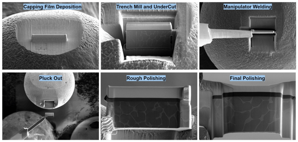
Standard Lamella Preparation
Series of six images illustrating stages in advanced TEM sample preparation: capping film deposition, trench milling and undercutting, manipulator welding, plucking out, rough polishing, and final polishing.
Application Examples
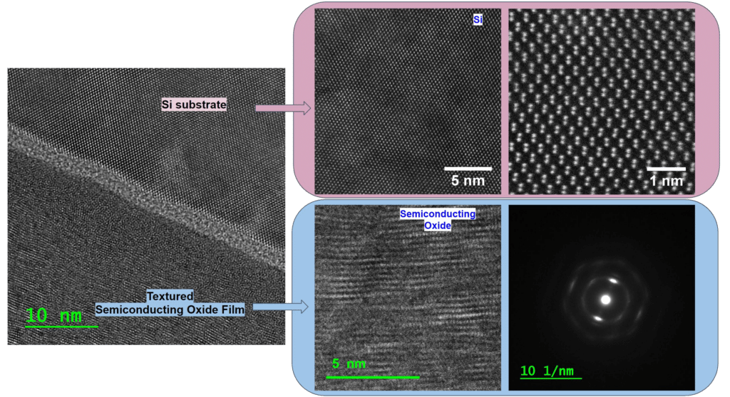
Sample: Semiconducting Oxide Film on Si FIB Application: Low voltage 2kV Ar polishing to produce damage free sample for HR-STEM imaging Sample Courtesy: Avalon Holographics Inc., Edmonton
Microscopic images reveal the Si substrate (upper panel) and a textured semiconducting oxide film (lower panel), featuring distinct nano-scale structures and electron diffraction patterns, achieved through advanced TEM sample preparation techniques.
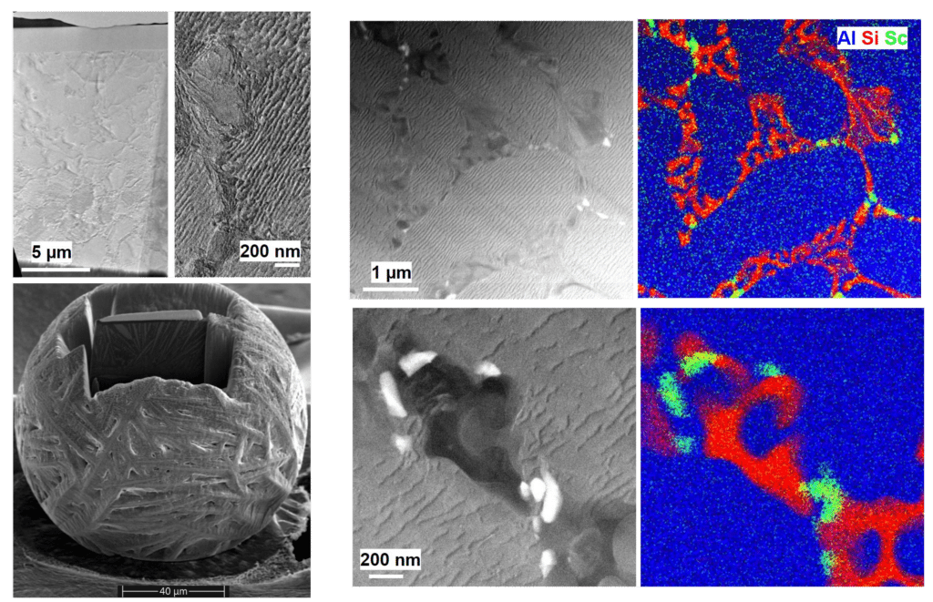
Sample: Rapidly solidified Al-10Si-0.4Sc droplets (atomized using Impulse Atomization) FIB Application: Flexible micromanipulation to pluckout samples from spheres Sample Courtesy: Akki Sahoo, Dr. Jonas Valloton and Prof. Hani Henein, Faculty of Engineering, University of Alberta; Abdoul-Aziz Bogno, Equispheres Inc., Ottawa
A collage of microscopic images, prepared with advanced TEM techniques, showcases various materials' textures and compositions with scale bars. The top right image features a color map, highlighting elements labeled as Al, Si, and Sc.
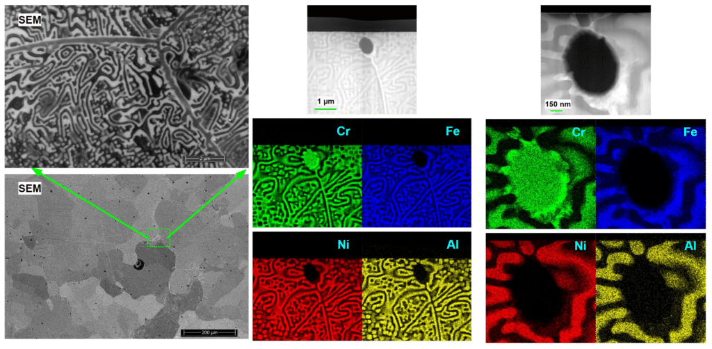
Sample: Al-Cr-Fe-Ni medium-entropy alloy (MEA) FIB Application: Mixed Pt/C capping film for effective protection for HEA/MEA materials Sample Courtesy: Guijiang Diao and Prof. Dongyang Li, Faculty of Engineering, University of Alberta
A series of SEM and color maps displaying material composition, with elements Cr (green), Fe (blue), Ni (red), Al (yellow) on a patterned surface. Focus is on a circular area, highlighting the precision in sample preparation for Advanced TEM analysis.
Sample: Intel Core i7 processor FIB Application: Inverted pluckout to reduce curtaining and damage in the regions of interest.
Advanced TEM images reveal semiconductor structures with ion beam detection, highlighting inverted pluck-out areas. Color coding indicates elements: Cu, Si, Ti, ensuring precise TEM sample preparation for detailed analysis.
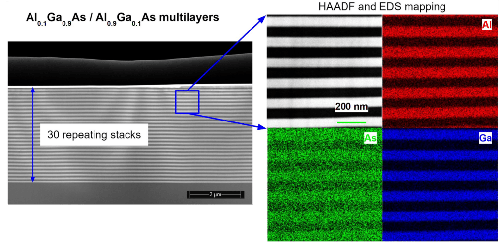
Sample: AlGaAs multilayers FIB Application: 90-degree pluckout (ion beam parallel to the layer stacks) to produce uniform thin thickness across all layers.
A semiconductor cross-section reveals layers of Al₀.₃Ga₀.₇As and Al₀.₄₅Ga₀.₅₅As on Si, with advanced TEM images and a diffraction pattern presented on the right, highlighting meticulous sample preparation techniques.Advanced TEM nanobeam diffraction images reveal crystallographic mismatch in Al[_x]Ga[_{1-x}]As/Al[_y]Ga[_{1-y}]As layers, complemented by a selected area electron diffraction pattern.Microscopic image of AlGaAs/AlGaAs multilayers displaying 30 repeating stacks. Includes HAADF and EDS mapping with highlighted elements: Al in red, As in green, Ga in blue. Advanced TEM sample preparation showcases intricate layer details for accurate analysis.
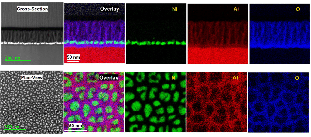
Sample: Nano-composite material (Ni nanoparticles in anodized Al) FIB Application: Flexible miro-manipulation to produce cross-sectional and plan-view lamellas Sample Courtesy: Dr. Matthew Nickel and Prof. Todd McMullen, Faculty of Medicine & Dentistry, University of Alberta
Advanced TEM cross-sectional and plan-view microscopy images reveal distributions of Ni, Al, and O with remarkable clarity. The cross-section shows stratified layers, while the plan-view features patchy clusters. Scale bars are set at 200 nm and 50 nm respectively.
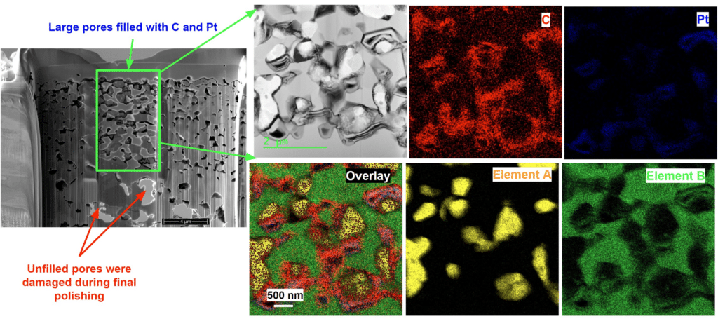
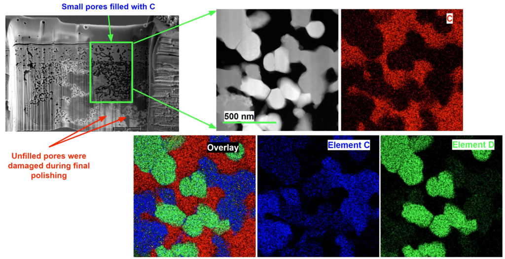
Sample: Porous solid oxide fuel cell FIB Application: Back-filling with in-situ GIS to prepare high quality samples from porous materials. Sample Courtesy: Prof. Douglas Ivey, Faculty of Engineering, University of Alberta
Microscopic images using advanced TEM reveal pores, element concentration maps, and overlays; highlighting small carbon-filled pores and unfilled, damaged pores.
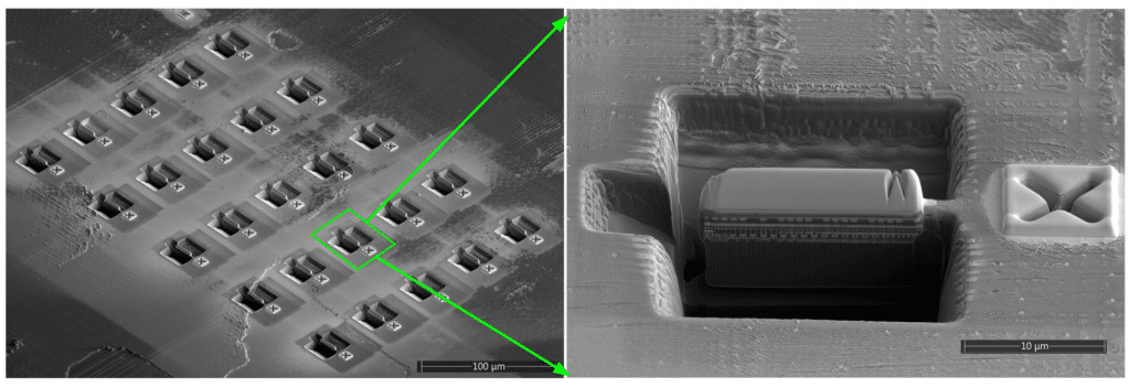
Sample: Intel Core i7 processor FIB Application: Fully automatic/unattended site preparation of 25 locations
A grayscale image showcasing a zoomed-in view of microstructures highlights an inset detailing a close-up of one microstructure, prepared using Advanced TEM techniques, featuring a rectangular shape inside a square cavity.
SAXS, GI-SAXS/WAXS are available on Bruker D8D+
The nanoFAB is pleased to announce that advanced Small-Angle X-ray Scattering (SAXS), Grazing-Incidence Small-Angle and Wide-Angle X-ray Scattering (GI-SAXS/WAXS) techniques are fully commissioned on the Bruker D8 DISCOVER Plus X-Ray Diffractometer and now open for user training.
SAXS utilizes small-angle x-ray scattering to quantify nano-scale density differences in a sample, which enables characterization of nanostructures in terms of the averaged particle sizes, shapes, distribution, pore sizes, characteristic distances of partially ordered materials, and much more. This is achieved by analyzing the elastic scattering behavior of X-rays when traveling through the material, recording their scattering at small angles (typically 0.1 - 10°).
The materials for SAXS analysis can be solid or liquid and they can contain solid, liquid or gaseous domains (so-called particles) of the same or another material in any combination. Not only particles, but also the structure of ordered systems like lamellas, and fractal-like materials can be studied. For thin films supported on solid substrates (such as glass or Si), derivatives of SAXS, namely GI-SAXS/WAXS can be used to characterize ordered structure/alignment within the films relative to the substrate surface, particularly molecular alignment/arrangement of polymer films. These methods are accurate, non-destructive and usually require a minimum of sample preparation. Applications are very broad, including colloids of all types, metals, cement, oil, polymers, plastics, proteins, foods and pharmaceuticals.
If you are interested in the SAXS, GI-SAXS/WAXS analysis, please submit a request (training or sample type) with sample details on LMACS. Our XRD team (Drs. Xuehai Tan and Nas Yousefi) will follow up and arrange sample analysis and training. If you have any questions, please feel free to contact Peng Li (Peng.Li@ualberta.ca) – the Characterization Group Manager.
Application Examples
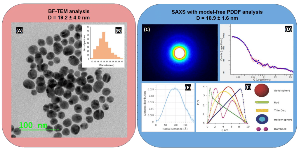
Sample: 20 nm Au NPs Sample preparation: in water (capillary tube) Analysis: SAXS Application: Size distribution analysis
Among several techniques to measure particle size, SAXS provides accurate, reliable and high throughput analysis with simple sample preparation. While TEM imaging based analysis provides direct visualization with very high spatial resolution, it requires proper sample preparation (well dispersed particles) and the result accuracy relies on the quality of particle intensity thresholding. SAXS analysis is less dependent on sample preparation and probes a large volume of samples, providing the most statistically relevant results.
Figure 1: (A) Bright-Field TEM image and (B) measured size distribution of the Au nanoparticles, diameter = 19.2 ± 4.0 nm. (C) 2D SAXS data measured with an evacuated flight tube (EFT) filled with vacuum. (D, E) SAXS data integrated into 1D and background subtraction: A model-free analysis based on Pair Distance Distribution Function (PDDF). The obtained result is indicative of an overall spherical particle shape with approximated diameter of 18.9 nm. (F) PDDF P(r) functions for geometric bodies, adapted from DOI 10.1088/0034-4885/66/10/R05
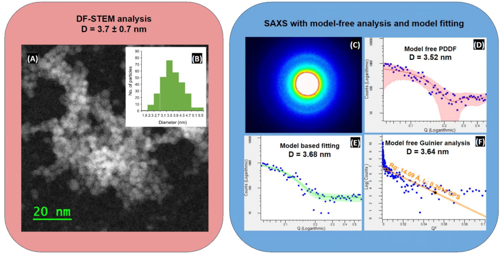
Sample: 3 nm Si QDs Sample preparation: in toluene (capillary tube) Analysis: SAXS Application: Size distribution analysis Sample Courtesy: Chuyi Ni and Prof. Jon Veinot, Department of Chemistry, University of Alberta
TEM imaging analysis can be very challenging to characterize particle size when particles are difficult to disperse and/or the particles give poor contrast, such as light-element quantum dots (QDs), e.g., Si or carbon QDs. SAXS can provide reliable size and shape structure determination, empowered by several data analysis / modelling methods and further advances in instrumentation.
Figure 2: (A) Dark-Field STEM image and (B) measured size distribution of Si QDs, diameter = 3.7 ± 0.7 nm. (C) 2D SAXS data measured with an evacuated flight tube (ETF) filled with vacuum. SAXS analysis results with model free and model fitting: (D) Model free PDDF, diameter = 3.52 nm; (E) a model-based fitting assuming polydisperse spheres with Schultz size distribution and no interaction, diameter = 3.68 nm; (F) model-free Guinier analysis, diameter = 3.64 nm.
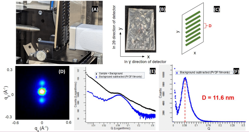
Sample: textured PVDF film Sample preparation: Freestanding film Analysis: SAXS Application: Internal periodical structures and orientation Sample Courtesy: Amanuel Abay and Prof. Anastasia Elias, Faculty of Engineering, University of Alberta
SAXS is useful not only for characterizing the size and shape of particles, but also for measuring structural information of partially or completely disordered systems. In the following example, SAXS analysis is utilized to study the internal repeating structure of a free-standing PVDF film.
Figure 3: (A) a photo of the SAXS setup, including X-ray collimator, the vertically mounted free-standing PVDF film, and the evacuated flight tube (EFT) that is attached to the 2D detector. (B) The orientation of the sample with respect to the 2theta and gamma directions of the 2D detector. (C) Illustration of the internal lamella orientation confirmed by the SAXS analysis. (D) 2D SAXS data marked with q values in both 2𝛉 and 𝞬 directions. (E) SAXS data integrated into 1D and background subtraction. (F) The measured q value suggests a repeated distance of 11.6 nm for the internal lamella.
Sample: Organic Photovoltaic (OPV) films (30 nm PEDOT + 250 nm P3HT:PCBM) Sample preparation: Spin-coated on ITO-coated glass substrate Analysis: GI-SAXS Application: Internal periodical structures and orientation Sample Courtesy: Prof. Jillian Buriak, Department of Chemistry, University of Alberta
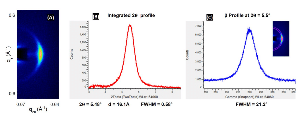
GI-SAXS is particularly useful to analyze domain size, interplanar spacings and orientation of small molecule/polymer thin films for photovoltaics, block copolymer thin films and inorganic/metal thin films for batteries. GI-SAXS analysis of an organic Photovoltaic film (P3HT:PCBM) measured an interplanar spacing d = 1.61 nm and their 2D distribution (both in-plane 2𝛉 and out-of-plan β).
Figure 4: (A) 2D GI-SAXS data marked with q values in both 2𝛉 and gamma directions; (B) Integrated profile in 2𝛉 direction and (C) Integrated profile in β direction.
Sample: PBTTT film (30 nm) Sample preparation: spin-coated on ITO-coated glass substrate Analysis: GI-WAXS Application: Internal periodical structures and orientation Sample Courtesy: Prof. Loren Kaake, Department of Chemistry, Simon Fraser University
Semiconducting polymers play an important role in advancing the field of printed and mechanically flexible electronics, such as flat panel displays and photovoltaic cells. Thin film transistors with thiophene-based polymer layers have demonstrated good field-effect carrier mobilities that are considered highly valuable across various applications. It is widely recognized that achieving high carrier mobility in these materials hinges on the precise molecular ordering, as charge movement depends on effective intermolecular electronic coupling. While the spacing of the molecular ordering and crystalline domains is too small for GI-SAXS, GI-WAXS provides an effective analysis.
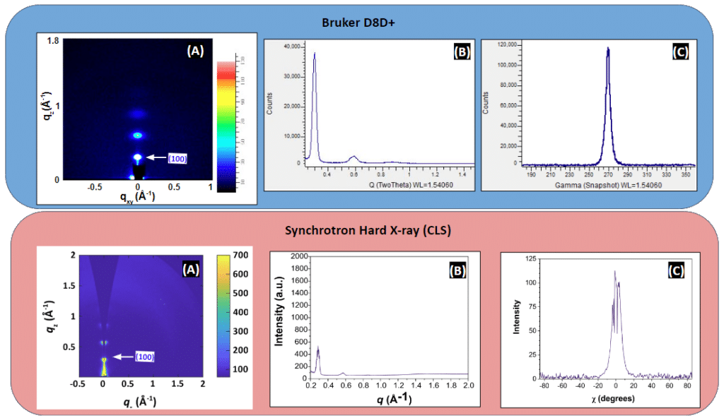
As shown in the figures below, typical GI-WAXS setups on the Bruker D8D plus (0.1 mm slit and a 0.3 mm Goebel mirror collimator, 0.17° incidence angle, and 145 mm sample-to-detector distance) effectively confirms the edge-on orientation of the polymer lamellas in a 30 nm PBTTT film on glass.
Compared to the results (available here) obtained from the Synchrotron Hard X-ray MicroAnalysis (HXMA) beamline (at the Canadian Light Source), the GI-WAXS analysis on the Bruker D8D plus provides equally informative results, but more accessible to general users.
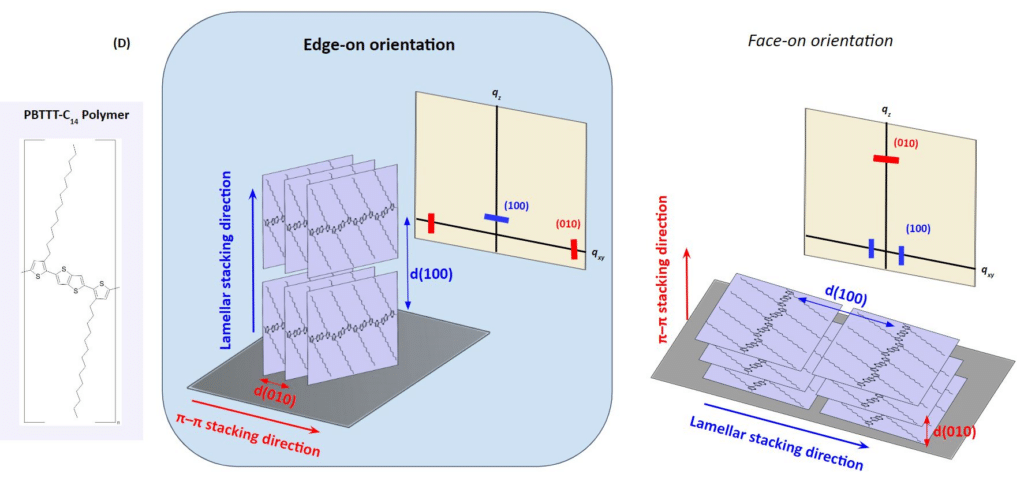
Figure 5: GI-WAXS results of PBTTT thin films measured on the Bruker D8D + and the Synchrotron Hard X-ray MicroAnalysis (HXMA) beamline of the Canadian Light Source. (A) Two-dimensional WAXS scattering data (B) 1D profile of the scattering intensity. (C) Azimuthal dependence of the scattering intensity. (D) The molecular structure of PBTTT and the schematic depicting PBTTT different molecular alignment within thin layers relative to the substrate surface: Edge-On and Face-On orientations. The arrangement of molecules within the cell is primarily qualitative and is not intended to provide a quantitative representation of the precise molecular packing specifics.
Broad Ion Beam (BIB) polishing for SEM/EDX/EBSD
The RES 102 system features:
Ion energy: 0.8 to 10 keV
Source current: Up to 4.5 mA
Stage Rotation: 0.6 to 10 rpm
Sample size SEM holder: max. Ø 25 mm × 12 mm
Prepared area SEM holder: max. Ø 25 mm
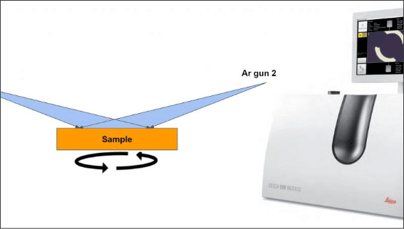
RES102 BIB Ion Milling System equipped with two Ar guns
Among general electron microscopy applications, Electron Backscatter Diffraction (EBSD) is a surface technique – typical probing depth is in the range of a few tens nm for a beam energy of 20 kV. Smooth and damage-free surface is critically important to obtain high quality EBSD data. Compared to conventional mechanical polishing techniques, which can result in very rough surfaces and a thick damaged layer, low energy beam at grazing incident angle and rotating stage on the RES102 can effectively polish the surface to reduce roughness and remove the damaged layer.
With the programmable recipes of flexible parameters (beam energy, beam current, incident angle, stage rotating speed), the RES102 BIB has produced very nice results for our users for EBSD analysis. See recent examples below.
Application Examples (EBSD)
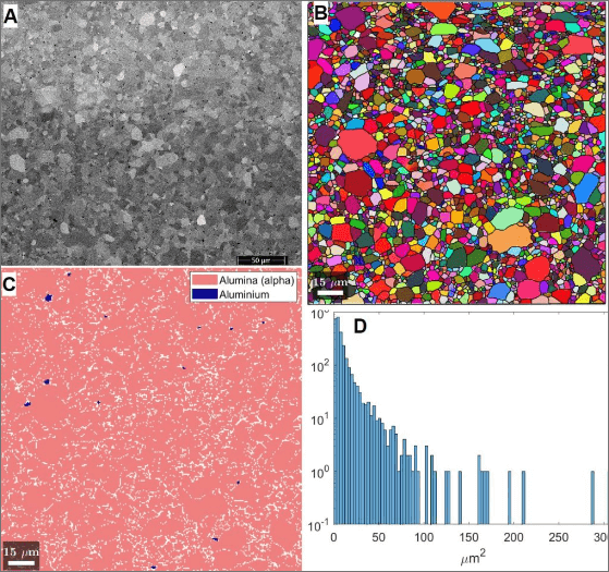
Sample: 3D printed Alumina for structural applications
Sample Courtesy: Cass (Haoyang) Li, Dr. James Hogan, Mechanical Engineering Department, Faculty of Engineering, University of Alberta
Ion Milling process:
8 kV, 3 mA, 3.5 degrees, 1.5 rmp for 120 mins
8 kV, 2 mA, 2.5 degrees, 1.5 rmp for 60 mins
EBSD mapping: 175 µm x 175 µm, stepsize 50 nm
(A) SEM image; (B) Orientation map; (C) Phase maps of Alumina and Aluminium; (D) Grain size distribution
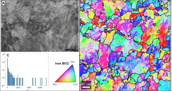
Sample: Rail Steel
Sample Courtesy: Stephen Okocha, Drs. Ben Jar and Michael Hendry, Mechanical Engineering Department, Civil and Environmental Engineering Department, Faculty of Engineering, University of Alberta
Ion Milling process:
8 kV, 3 mA, 2.5 degrees, 1.5 rmp for 60 mins
6 kV, 2 mA, 2.5 degrees, 1.5 rmp for 60 mins
EBSD mapping: 300 µm x 300 µm, stepsize 250 nm
(A) SEM image; (B) Orientation map; (C) Grain size distribution
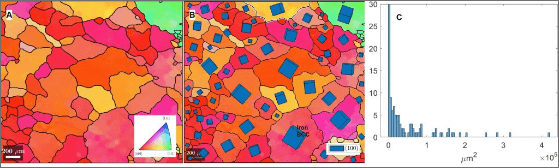
Sample: Al-Cr-Fe-Ni medium-entropy alloy (MEA)
Sample Courtesy: Guijiang Diao, Dr. Dongyang Li, Chemical and Materials Engineering Department, Faculty of Engineering, University of Alberta
Ion Milling process:
8 kV, 3 mA, 3.5 degrees, 1.5 rmp for 60 mins
5 kV, 2 mA, 2.5 degrees, 1.5 rmp for 60 mins
EBSD mapping: 2500 µm x 1500 µm, stepsize 500 nm
(A) Orientation map; (B) Crystal unit cell orientation and (C) Grain Size Distribution
The RES102 ion milling system is now available to general users for both staff analysis and user training. Any users interested in getting trained on this tool or staff analysis should submit a request on LMACS. If you have any questions, please contact the tool managers Drs. Nas Yousefi and Shihong Xu or Peng Li – the Characterization Group Manager

![Advanced TEM nanobeam diffraction images reveal crystallographic mismatch in Al[_x]Ga[_{1-x}]As/Al[_y]Ga[_{1-y}]As layers, complemented by a selected area electron diffraction pattern.](https://www.nanofab.ualberta.ca/wp-content/uploads/2025/02/06b-Al-Ga-As-1024x410.png)