Field alignment now available on the Heidelberg MLA150
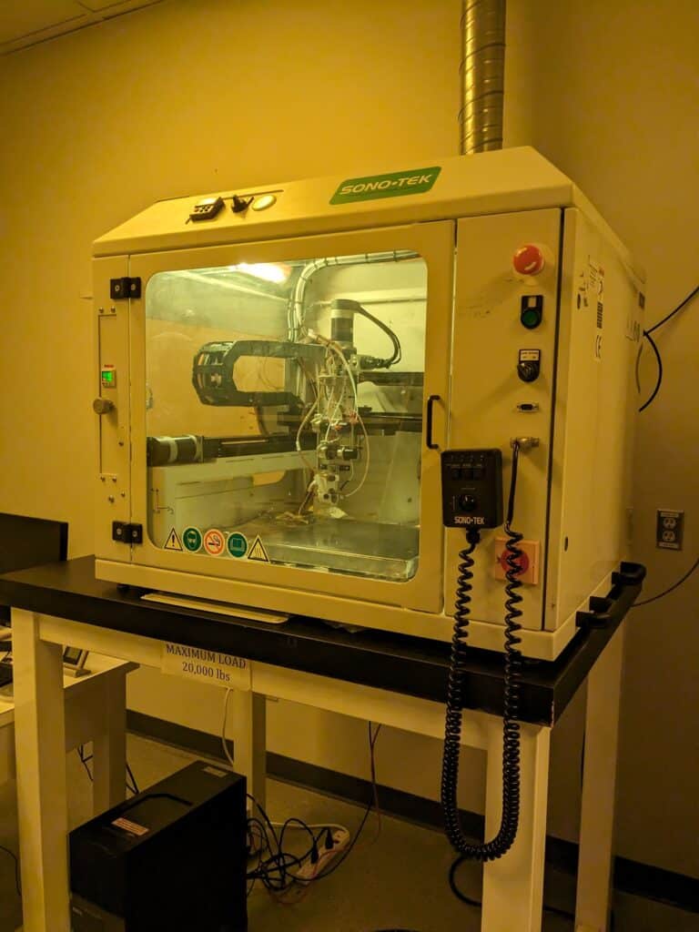
The Heidelberg MLA150, our direct-write laser lithography system, is known for its outstanding performance when aligning a new design to a patterned wafer. Nominally the system is capable of better than ±500 nm global alignment precision in both X- and Y-directions (for topside, ±1 μm for backside), typically surpassing that and producing results in the ±300 nm range. However, depending on factors such as stress build-up on wafers due to deposited materials, this precision may become compromised and produce both worse alignment overall as well as non-uniform precision (i.e., varying die-to-die alignment precision).
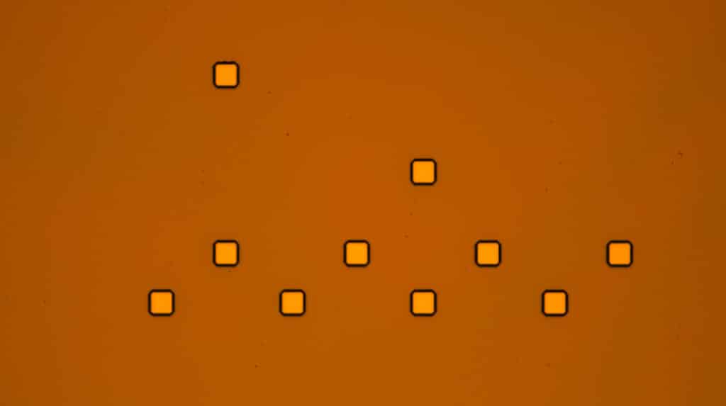
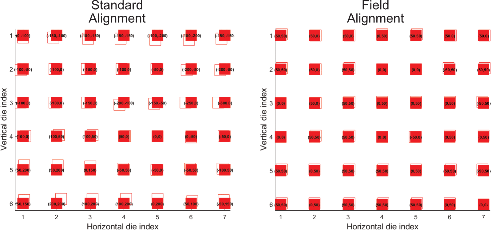
To overcome the limitations caused by using a single, global alignment for a whole wafer, we now have the option to perform local alignment on each die. This new method, as evidenced by the image below, greatly improves alignment precision on each die, reducing both the overall offset and the die-to-die variation. In this demo, standard alignment (left) shows offsets in the ±300 nm range. While all dies are within specification, the offset still varies by up to 500 nm die-to-die. On the other hand, field alignment (right) greatly improves the results, such that all dies exhibit offsets in the ±50 nm range (i.e., the resolution of the verniers used for this test).
This improved precision does come at the cost of longer exposure times, however, since the system now has to scan and measure alignment marks for each die being patterned. However, this is a reasonable cost to pay when poor alignment is detrimental to device performance. Please note that this new technique is only available for topside alignment—it cannot be used for backside alignment due to the requirements for this procedure.
If you are interested in using this new field alignment feature, a new document detailing the procedure is available by the tool, and in our Knowledge Base. Also, please do not hesitate in submitting a training request via LMACS if you wish to get hands-on training. For more information, please contact Gustavo de Oliveira.