Optical Emission Interferometry (OEI) in the Plasma-Therm Versaline PECVD

Overview

In plasma-enhanced chemical vapour deposition (PECVD) tools, the deposition rate of deposited films can often fluctuate with relative gas concentrations, material build-up on the chamber walls, and other mechanisms that make timed depositions inconsistent. To combat this problem, a simple technique called Optical Emission Interferometry (OEI) can be used. OEI provides a more robust form of deposition control based on the interference of light reflected off of the growing film to precisely hit target film thicknesses.

OEI uses similar principles to other interferometric tools like the Filmetrics F50-UV; the intensity of light at a single wavelength reflected off of a thin film will vary depending on the wavelength of light and the optical thickness of the film. This is due to the relative phase difference between light reflected off the top surface of the film and at the film-substrate interface, i.e., conditions of constructive and destructive interference (shown in Fig. 1). Across a broad spectrum of wavelengths, this can be used to fit to both refractive index and film thickness robustly (as Filmetrics does). However, if the intensity of light reflected off of a growing film is recorded continuously, the intensity at a "single" wavelength will oscillate approximately sinusoidally as the thickness increases (satisfying constructive and destructive interference conditions at specific thicknesses)—this is the fundamental premise of OEI. By noting when the extrema occur during film growth, the period of this oscillation (T) can be used to measure the deposition rate of the film, since T is set by the phase conditions for constructive/destructive interference. T = λ/(2n); where λ is the wavelength of interest and n is the refractive index of the material at this wavelength.
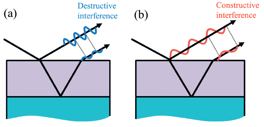
Diagram illustrating (a) destructive and (b) constructive interference, incorporating the principles of Optical Emission Interferometry. Two waves reflect off surfaces, with destructive showing out-of-phase and constructive in-phase interactions.
Figure 1. Phase conditions for destructive and constructive interference of light reflected off of a thin film, from H. G. Tompkins, and J. N. Hilfiker, Spectroscopic Ellipsometry: Practical Application to Thin Film Characterization (Momentum Press, 2016).

To use OEI in the Plasma-Therm Versaline PECVD, light produced by the plasma is reflected off of the growing film and collected by a spectrometer centred above the wafer for plasma monitoring. The Plasma-Therm EndpointWorks software package is then used to monitor the evolution in time of the spectral intensity emitted from the plasma within a narrow range of wavelengths. Choosing a range that encompasses an emission line of a typical gas/radical species within the plasma produces the oscillatory data shown in Fig. 2. Values of T are calculated based on known values of n and λ to give an estimate of the deposition rate based on the spacing of the extrema. Thus, in order to function correctly, each OEI recipe requires the user to have knowledge of both the growing film (single wavelength refractive index) and of typical optical emission lines (usable wavelengths) within the plasma.
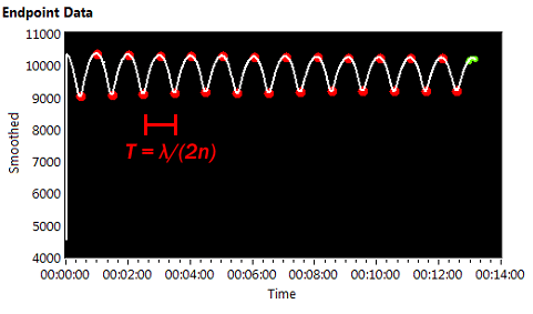
Graph titled "Endpoint Data" shows an oscillating white line with red and green highlights, likely depicting Optical Emission Interferometry data. The X-axis is time and the Y-axis is smoothed data. A red notation reads "T = λ/(2n)" with a horizontal bracket, possibly showcasing Plasma-Therm analysis.
Figure 2. EndpointWorks Thickness Detector data for a growing SiO2 film.

Wavelength choice

The choice of what wavelength to use for OEI depends on the chemistry of the plasma in question, since each gas/radical species emits light at different wavelengths (depending on its electronic transitions), and thus the available wavelengths will differ for each recipe. Potential emission lines are further limited if the gas species characteristic of an emission line is consumed during the reaction. The intensity of these reactant emission lines will fluctuate as the film grows and as the local gas concentration changes. In contrast, the intensity of an emission line of an inert gas (He, Ar, or N2 are often used to dilute the reactants) will be much more stable, and will provide a reduction in noise in the reflected light. This leads to a more clearly defined periodic signal, where the extrema can be easily identified in software. Additionally, since variation in T is linear with the wavelength of light used, the choice of shorter wavelengths will reduce the period of oscillation, lending the OEI method more sensitivity and flexibility to accurately measure thinner films. Note, for films that are optically absorbing (e.g. a-Si and Si-rich nitrides), the film will absorb more strongly at shorter wavelengths, decreasing the amplitude of the oscillation as the film grows. Ultimately, this decay reaches a point where extrema cannot be identified past a certain thickness. A general rule of thumb is to choose the shortest wavelength inert gas emission line that is not strongly absorbed by the depositing film. A typical spectrum collected during deposition is shown in Fig. 3, where a N2 emission line at ~333 nm is highlighted, being suitable for the gas chemistry involved. For more details on choosing an emission line appropriate for your deposition, please see the Plasma-Therm Versaline PECVD OEI recipe development How-To on the nanoFAB's Confluence Knowledge Base.
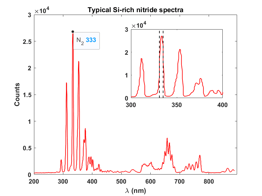
Graph showing Si-rich nitride spectra with wavelength (nm) on the x-axis and counts on the y-axis, using Plasma-Therm's Optical Emission Interferometry. Main peak at 333 nm. Inset shows detailed view of 300-400 nm range with multiple peaks.
Figure 3. Typical plasma emission spectrum (as measured on the Versaline's integrated Ocean Optics spectrometer) for the deposition of Si-rich nitride. Inset: full-width at half-max (dashed lines) of the N2 emission line centred at ~333 nm.

OEI controlled deposition recipes are currently qualified for SiO2 Dep ("OEI SiO2 Dep") and Stoichiometric Nitride ("OEI Stoichiometric Nitride") recipes, with an OEI recipe in progress for the Si-Rich Nitride. For user-developed films that differ from these established recipes, users are welcome to qualify their own OEI recipes following the Step-by-step instructions in the linked OEI recipe development How-To. If you encounter problems setting up your OEI recipe on EndpointWorks, please contact Tim Harrison (tr1@ualberta.ca).
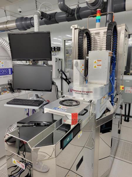
Plasma-Therm Versaline PECVD now available

Thin films available for deposition include:

  • a-Si (amorphous silicon)
  • SiNx (Si-rich and stoichiometric nitride)
  • SiO2 (silicon dioxide)
  • SiOxNy (silicon oxynitride)

Through its user-friendly software, the Plasma-Therm Versaline PECVD offers robust recipe control for tuning parameters such as refractive index, composition, and film stress. Currently available process and carrier gases are: SiH4 (100%), NH3, N2O, H2, Ar, He, and N2.

System features of the Plasma-Therm Versaline PECVD:

EndpointWorks is a multi-functional endpoint detection package for optical emission interferometry (OEI) and optical emission spectroscopy (OES) recipe control. OEI provides real-time deposition rate information and thickness control, while OES uses spectral information in the plasma to decrease the time required for clean cycles.

Typical uniformity results and optical constants for standard recipes/materials

a-Si

Recipe name: a-Si Dep

Diagram of a circular sample with color gradient from green to blue, produced using Versaline PECVD technology, showing various statistics including min, max, mean, and standard deviation values.

Silicon nitride

Recipe name: Stoichiometric Nitride Dep

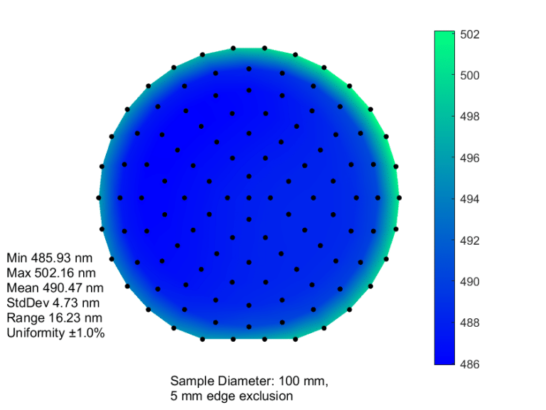
A color map of a circular sample created via PECVD displays gradient hues from blue to green, with black data points spread across the surface. A legend marks values from 490 to 502, while text on the left offers statistical data.
A colour map of a circular sample created via PECVD displays gradient hues from blue to green, with black data points spread across the surface. A legend marks values from 490 to 502, while text on the left offers statistical data.

Recipe name: Si-rich nitride Dep

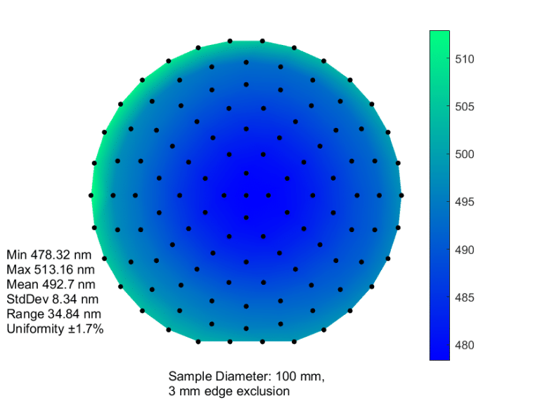
A circular, multicolored gradient map featuring data points from 480 to 510 created using Versaline technology. Text lists statistical measurements such as minimum, maximum, mean, standard deviation, and range values.

SiO2

Recipe name: SiO2 Dep

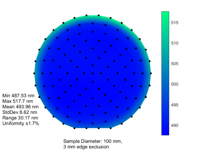
The image showcases a color-coded circular chart featuring statistics like minimum, maximum, mean, standard deviation, range, and uniformity. Using the Plasma-Therm Versaline PECVD system, the sample has a 100 mm diameter with a 3 mm edge exclusion for precise measurements.

Film modification and process trends

Plasma-Therm boasts an extensive process library, which may be consulted to aid users in the modification of our standard recipes for specific applications. Some trends within the typical parameter space for these recipes are shown below.

a-Si trends

While the nanoFAB standard a-Si film is reasonable for most applications, Plasma-Therm has provided the nanoFAB with a second a-Si recipe based on He-dilution that can be tuned to easily adjust the deposited film stress. See the table below for a brief comparison between the process parameters of this recipe and the nanoFAB standard recipe (a-Si dep):

Parametera-Si depHe-dilution
RF power (W)2025
Deposition pressure (mTorr)600900 to 1200
SiH4 flow rate (sccm)2550
He flow rate (sccm)01000
Ar flow rate (sccm)14000
Lower electrode temperature (°C)250140
Upper electrode temperature (°C)175140

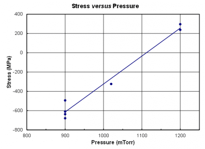
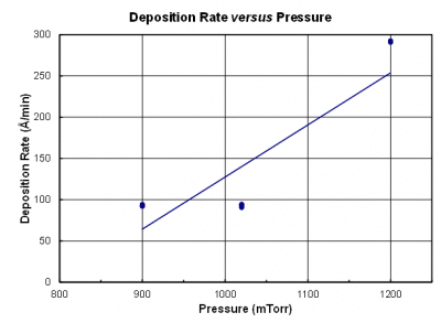
This He-dilution recipe exhibits the following process trends:

Graph of stress (MPa) versus pressure (mTorr) using PECVD on a Plasma-Therm system shows an upward trend from -600 MPa at 900 mTorr to 200 MPa at 1200 mTorr, with one outlier near 1000 mTorr.
Graph titled "Deposition Rate versus Pressure" from a Plasma-Therm PECVD system, showing a line with points at (900, 100), (1050, 200), and (1200, 300) on a grid. X-axis: Pressure (mTorr), Y-axis: Deposition Rate (Å/min).

If you are interested in using this a-Si deposition recipe, please contact the primary tool trainer, Tim Harrison (tr1@ualberta.ca), for details.

Please note that regardless of the a-Si deposition recipe used, OEI for endpoint detection does not work well due to the high optical absorption of a-Si.

SiON trends

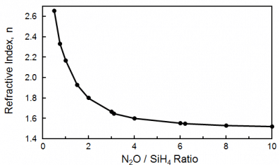
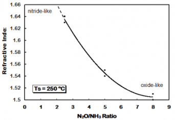
The typical reactions used in the Plasma-Therm Versaline PECVD for the deposition of nitride films allows for the deposition of a silicon oxynitride (SiOxNy) by the modification of gas ratios and other deposition parameters. Oxynitride is a promising material that has been investigated for the development of optical components such as integrated waveguides, anti-reflective coatings, interferometers, filters, couplers, and splitters due to its tunable optical and mechanical properties. Such properties can be tailored by simultaneously adjusting both the N2O / SiH4 and N2O / NH3 ratios when depositing a film using a plasma chemistry of SiH4, N2O, and NH3. Depending on the application, films that are nearly pure silicon, primarily oxides, or even stoichiometric nitrides can be deposited. These films follow the general trends below:

Graph illustrating a decreasing refractive index as the N₂O/SiH₄ ratio rises from 0 to 10, utilizing Plasma-Therm's Versaline PECVD system.
The graph, utilizing Plasma-Therm's cutting-edge PECVD technology, illustrates the refractive index versus N₂O/NH₃ ratio. It depicts a curve shifting from 1.66 nitride-like to 1.52 oxide-like at Ts = 250°C on a Versaline system.

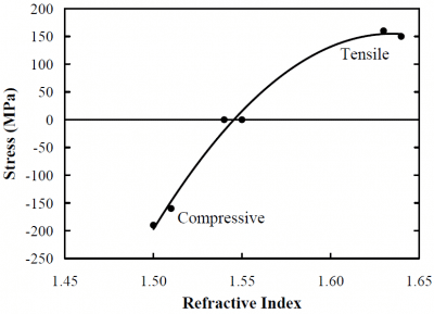
Meanwhile, the film stress is tied to the refractive index of the film (i.e. how oxide-like or nitride-like the film is):

Graph illustrating stress (MPa) vs. refractive index, created using PECVD on a Plasma-Therm Versaline system. Stress varies from -250 MPa (compressive) to 200 MPa (tensile) as the refractive index increases from 1.45 to 1.65.

SiO2 trends

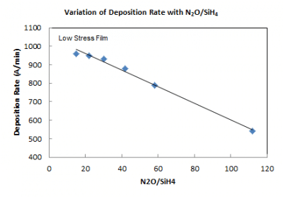
By utilizing a similar gas chemistry to that used for oxynitrides, a pure oxide film can be deposited. Such films have many uses in semiconductor and micro-optics including use as insulating layers for integrated circuits, low refractive index optical films, encapsulation, passivation layers, and more. Each application tends to emphasize different film properties, including (but not limited to) uniformity, deposition rate, film stress, refractive index, and wet etch rate, which can be tuned in the deposited film by the adjustment of process parameters.

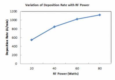
For the Plasma-Therm Versaline PECVD deposited oxide:

The graph illustrates how the deposition rate in a PECVD process varies with the N2O/SiH4 ratio. Using Plasma-Therm's Versaline, the rate decreases linearly from 950 Å/min at a ratio of 30 to 200 Å/min at 110.
Graph showing deposition rate in Å/min increasing linearly with RF power in watts, depicted by a line through data points at 20, 40, 60, and 80 watts using Plasma-Therm's versatile PECVD systems.


PECVD vs. LPCVD

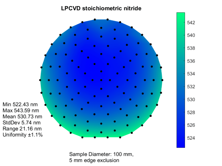
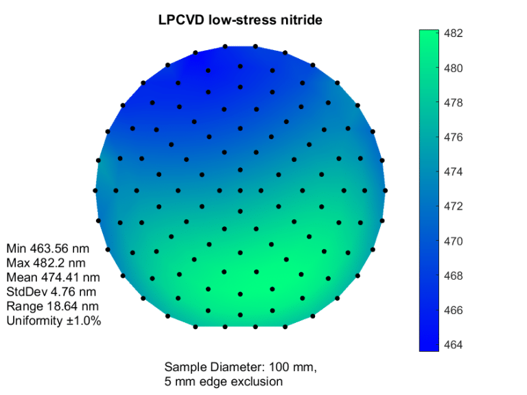
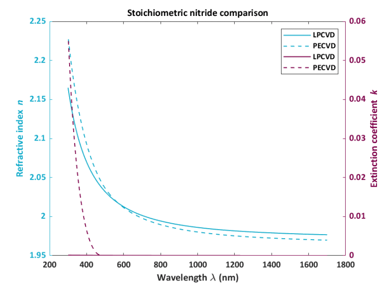
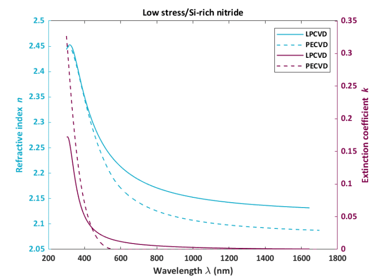
The addition of the Plasma-Therm Versaline PECVD offers the nanoFAB community the ability to produce high quality SiNx films by depositions performed at lower temperatures and over much shorter timescales than typical Low Pressure Chemical Vapour Deposition (LPCVD). The Plasma-Therm Versaline PECVD is also capable of producing low-stress stoichiometric nitrides that are nearly impossible to produce via LPCVD. Shown below are comparisons between the typical optical constants of the films produced by the Tystar LPCVD Tube furnace (Tube 2) and those produced by the Plasma-Therm Versaline PECVD. Typical uniformity maps for LPCVD nitrides are also given for comparison to the uniformity maps shown above for Plasma-Therm deposited films.

A heat map of LPCVD stoichiometric nitride wafer, possibly enhanced by Plasma-Therm technology, shows thickness in nanometers. It features statistics like minimum, maximum, mean, standard deviation, range, and uniformity percentages.
A circular heatmap displays thickness variation in LPCVD low-stress nitride, ranging from 464 to 482 nm, with stats: min 463.56 nm, max 482.2 nm, mean 474.41 nm. This analysis complements Plasma-Therm's advanced capabilities on a sample diameter of 100 mm.
Graph comparing stoichiometric nitride: Refractive index (n) in blue and extinction coefficient (k) in pink over wavelengths (200-1800 nm) for LPCVD and PECVD methods, showcasing Versaline technology by Plasma-Therm, with a legend.
Graph depicting the refractive index (n) and extinction coefficient (k) of Si-rich nitride versus wavelength (nm). Distinct lines illustrate results from LPCVD and Versaline PECVD methods, highlighting Plasma-Therm's precise PECVD measurements.
MethodRecipeTypical stress (MPa)Uniformity over 100 mm Ø wafer (%)
LPCVDStoichiometric10001.1
PECVDStoichiometric-15 to -400.8
LPCVDLow-stress100 to 2501.0
PECVDSi-rich2001.7

Basic training on the Plasma-Therm Versaline PECVD is now available to all nanoFAB users via training requests submitted on LMACS. If you have any questions about the capabilities of the Plasma-Therm Versaline PECVD, please do not hesitate to contact Tim Harrison (tr1@ualberta.ca) or Aaron Hryciw (ahryciw@ualberta.ca).


Links

Recipe information pages

Amorphous silicon
Si-rich nitride
Stoichiometric nitride
Silicon dioxide