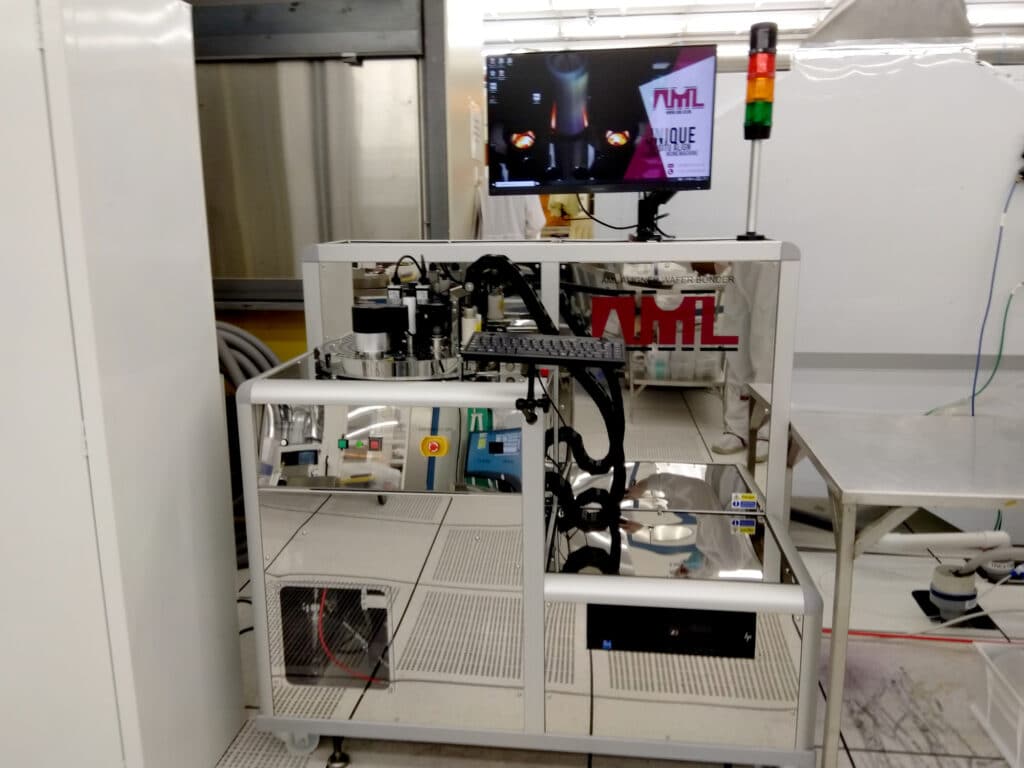
The nanoFAB is pleased to announce an upgrade to our wafer bonding and packaging area, with the recent installation of a wafer bonder from Applied Microengineering Ltd (AML). The AWB-04 wafer aligner-bonder from AML offers a wide range of bonding techniques and process flexibility. Of particular note is its in situ alignment capability, allowing users to verify correct alignment as the wafers are being brought into contact.
Bonding techniques include:
Anodic (borosilicate glass to Si)
Direct (Si to Si)
Eutectic (Si to Si or Si to glass with intermediate metal layer)
Thermocompression (bonding between metal films deposited on both substrates)
Other custom bonding techniques
Technical features:
Up to 150 mm wafer sizes (100 mm and 150 mm hardware available)
In situ alignment (visible and IR) with 1 µm accuracy; manual and automatic (image recognition) alignment procedures available
High vacuum (10-6 Torr)
Wafer separation of 30 mm
Independent platen temperature control, up to 560 °C
Radical activation (RAD) for in situ surface cleaning and activation
Bonding forces up to 40 kN
Anodic bonding voltages up to 2.5 kV, current limits up to 8 mA
Triple-stack anodic bonding
Wafer edge clamping (no contact on bonding surfaces)
Application Examples
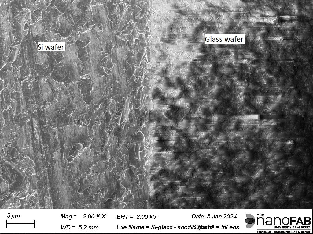
Anodic Bond: borosilicate glass to Si
Cross-sectional SEM (left) and TEM (right) images of bonding interface.
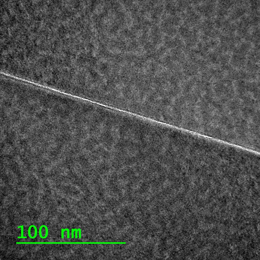
Si–Si Direct Bond: in situ RAD + low-temperature anneal
TEM images of the bonding interfaces of silicon wafers after a low-temperature (250 °C) anneal performed in the AWB-04 chamber without breaking vacuum. The thin amorphous native SiO2 layer can be seen along the interface.
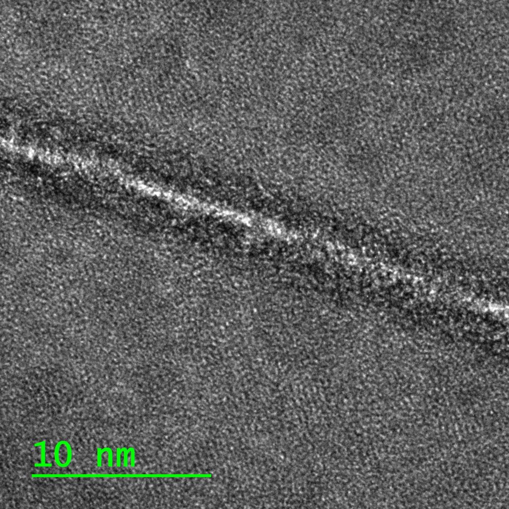
Si–Si Direct Bond: in situ RAD + external high-temperature anneal
TEM images of the bonding interfaces of silicon wafers after a high-temperature (1100 °C) anneal performed in Tystar General Anneal (Tube 6). The thin amorphous native SiO2 layer can be seen along the interface, but has diffused into the bulk Si layer.
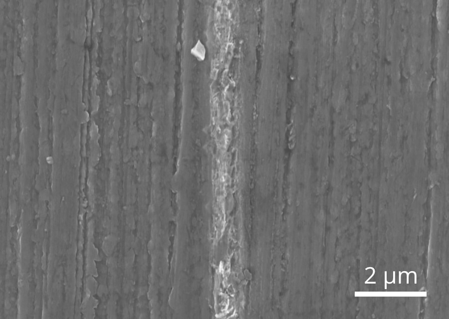
Au–Au Thermocompression Bond: Si to Si with Au interlayers
SEM images of silicon wafers bonded via Au–Au thermocompression bonding: full wafer cross-section (left) and close-up of bond interface (right). Patterned Au films are deposited on Si wafers and bonded using moderate temperatures (~300 °C) and high pressures (~7.5 MPa). Images courtesy of Jones Microwave Inc. and RM3.
If you are interested in using the AML wafer bonder in your work, please submit a request through LMACS to receive training. If you have any questions, please feel free to contact Scott Munro or Aaron Hryciw.
Kurt J. Lesker 150LX ALD system now open for training
The nanoFAB is pleased to announce that our newly installed and commissioned KJLC 150LX Atomic Layer Deposition system is now fully operational and available for training to all nanoFAB users. The ALD offers excellent uniformity and controlled growth of a variety of films on an atomic scale. Its high-vacuum load-lock and UHV-type sealing, combined with near-constant high-purity Ar flow, enable high-purity process conditions and excellent quality films.
Main system features include:
Single wafer transfer load-lock
Substrate heating up to 500 °C
150 mm platen, with an available carrier for samples <150 mm
Thermal and plasma-enhanced (PE-ALD) processes available
In situ film growth monitoring using Film Sense FS-1EX multiwavelength ellipsometer
The KJLC 150LX ALD is available to users for self-use (after training) and fee-for-service work. Any users interested in getting trained on this tool should submit a training request via LMACS. If you have any questions, please contact Aaron Hryciw (ahryciw@ualberta.ca) or Scott Munro (smunro@ualberta.ca).
Silicon etch processing
Recently, the nanoFAB installed and qualified a new, state-of-the-art silicon etch system from Oxford Instruments. The Oxford Estrelas ICPRIE system is capable of performing high-rate Si etch processes using the switched Bosch process, as well as thin-film silicon etches on the nanometre scale. Also equipped is a cryogenic process, in which smooth sidewalls are obtained by etching using SF₆ and O₂ at cryogenic temperatures.
Below are some SEM images depicting examples of typical Si etch processes performed using the Estrelas; more details about these processes can be found here. For further information or to enquire about tool usage, please contact Aaron Hryciw (ahryciw@ualberta.ca).
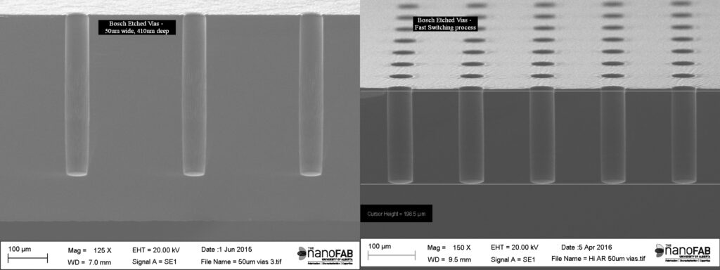
Bosch deep Si etching
High-rate (left) and smooth-sidewall (right) Bosch processes available for deep Si etching.
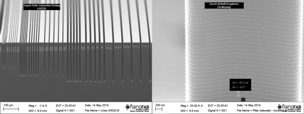
Bosch etching effects
Aspect ratio dependent etch rate (left) and sidewall scallops (right).
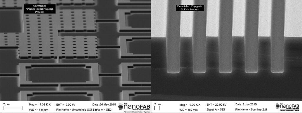
Unswitched Si etching
Use an unswitched etch process for thin Si device layers where sidewall smoothness is paramount.