Field alignment now available on the Heidelberg MLA150
The Heidelberg MLA150, our direct-write laser lithography system, is known for its outstanding performance when aligning a new design to a patterned wafer. Nominally the system is capable of better than ±500 nm global alignment precision in both X- and Y-directions (for topside, ±1 μm for backside), typically surpassing that and producing results in the ±300 nm range. However, depending on factors such as stress build-up on wafers due to deposited materials, this precision may become compromised and produce both worse alignment overall as well as non-uniform precision (i.e., varying die-to-die alignment precision).
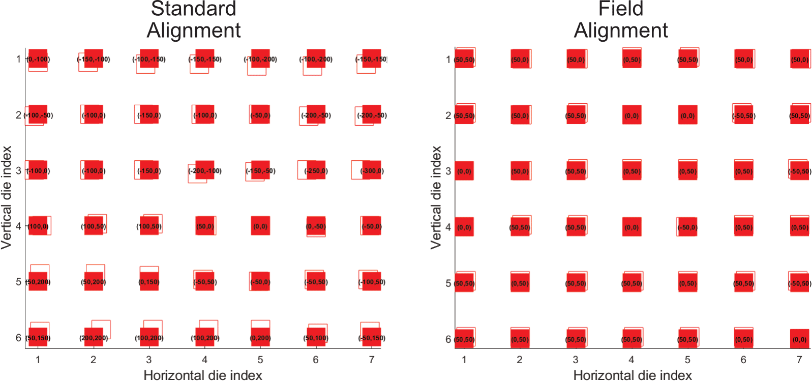
To overcome the limitations caused by using a single, global alignment for a whole wafer, we now have the option to perform local alignment on each die. This new method, as evidenced by the image below, greatly improves alignment precision on each die, reducing both the overall offset and the die-to-die variation. In this demo, standard alignment (left) shows offsets in the ±300 nm range. While all dies are within specification, the offset still varies by up to 500 nm die-to-die. On the other hand, field alignment (right) greatly improves the results, such that all dies exhibit offsets in the ±50 nm range (i.e., the resolution of the verniers used for this test).
Left: Standard (global) alignment. Right: Field alignment. Vertical and horizontal axes indicate the die index and its relative position on the test sample (not to scale). Each die is labeled with its respective (X,Y) offset in nm, with solid squares marking nominal position and red outlines marking the offset position. If the squares overlap at all, this represents "in-spec" alignment.
This improved precision does come at the cost of longer exposure times, however, since the system now has to scan and measure alignment marks for each die being patterned. However, this is a reasonable cost to pay when poor alignment is detrimental to device performance. Please note that this new technique is only available for topside alignment—it cannot be used for backside alignment due to the requirements for this procedure.
If you are interested in using this new field alignment feature, a new document detailing the procedure is available by the tool, and in our Knowledge Base. Also, please do not hesitate in submitting a training request via LMACS if you wish to get hands-on training. For more information, please contact Gustavo de Oliveira.
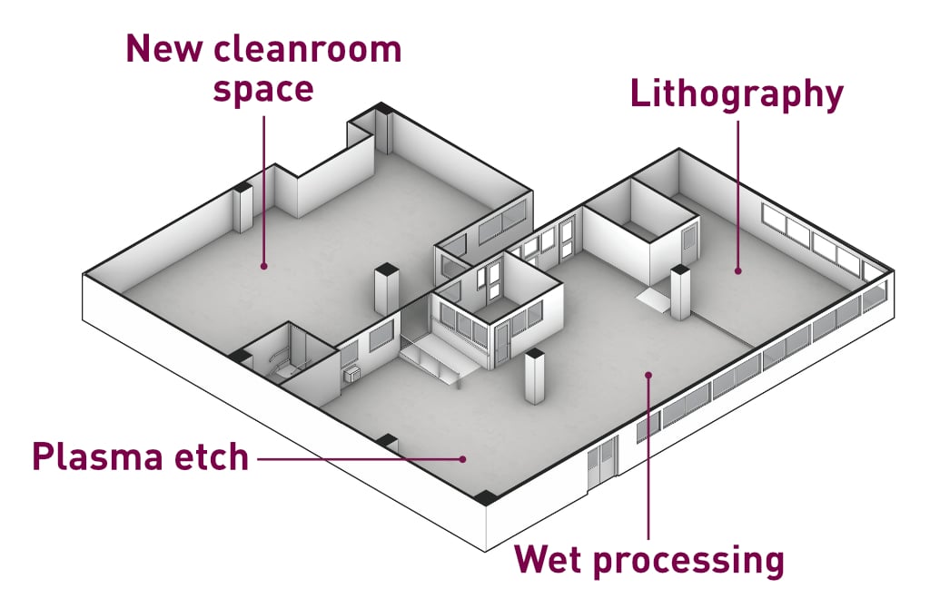
nanoFAB Unveils Cleanroom Expansion
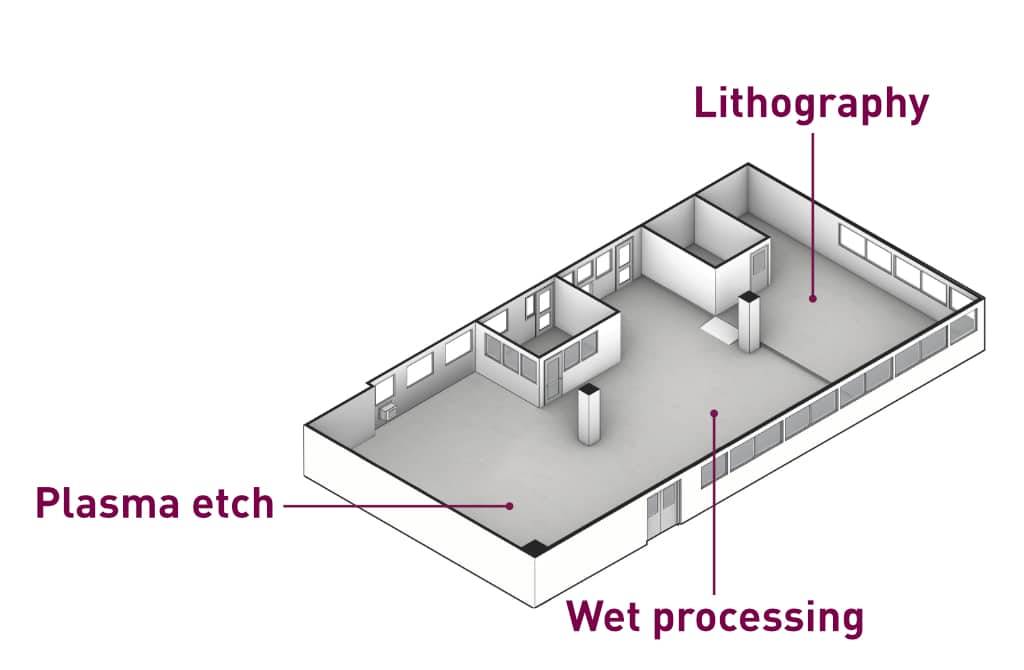
The nanoFAB has completed a large cleanroom expansion, marking a significant milestone in our 25-year history. This expansion represents a strategic investment in supporting the commercial and academic growth of semiconductor manufacturing and materials characterization at the nanoFAB. Through this expansion we are firmly establishing our role as a regional and national contributor to academic and commercial technology developments.
The nanoFAB is an open-access centre specializing in academic research and industry development in micro/nano fabrication and characterization. We provide training and access to over $100M in advanced state-of-the-art equipment and infrastructure to support hundreds of academic and industrial groups across Canada.
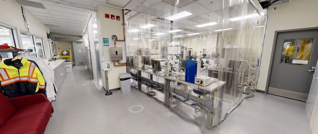
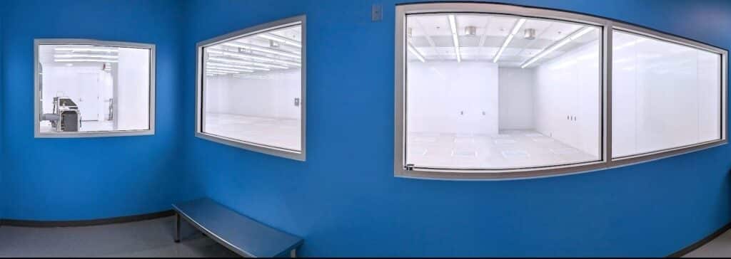
Original nanoFAB lab prior to cleanroom expansionNew nanoFAB cleanroom lab
This critical infrastructure upgrade is set to deliver substantial benefits:
Enhanced Capabilities and Capacity: The expansion directly addresses increased demand for industry hiring and growth, constrained by the lack of space for manufacturing activities. This new cleanroom space will allow for the installation of new equipment, enable hiring of new industrial employees, and create enhanced training opportunities for post-secondary students—boosting productivity, while filling capability gaps that will facilitate industry scale-up and research innovation activities in semiconductor device fabrication.
Driving Economic Diversification: The nanoFAB plays a vital role in fostering economic diversification and entrepreneurship, through providing access state-of-the-art capabilities allowing for technology development. This expansion will further support the development of high-value semiconductor manufacturing, particularly in areas such as energy, advanced electronics, sensing, and quantum systems. It aligns with our goal of strengthening innovation in Alberta and Canada by supporting a critical and growing mass of R&D activities.
Training the Next Generation of Talent: The nanoFAB is a crucial training ground for in-demand talent with hands-on experience in semiconductor manufacturing and materials characterization. This expansion will continue to support the development of highly skilled engineers, scientists, and technicians. The skills developed at the nanoFAB support a growing industry that contributes to economic diversification and the expansion of high-value manufacturing in Canada.
Strengthening Research and Innovation: The expanded cleanroom aligns with our strategic goals of attracting and retaining talent, developing open-access, sustainable infrastructure, and being able to support the growth of research, teaching, and commercialization activities within the University of Alberta. It also supports our broader goals of building a resilient local technology ecosystem that supports the scale-up of innovative hardware manufacturing capabilities.
Our cleanroom expansion, coupled with our ongoing support from industry partners and provincial and federal governments, underscores our strong commitment to being a catalyst for translating laboratory discoveries into high-value commercial outcomes, driving innovation and economic prosperity for Alberta and Canada.
For enquiries regarding this expansion, please contact nanofab@ualberta.ca.
Career Opportunity - Hyperlume Inc.
The nanoFAB is pleased to post the following two Front End Process Engineer career opportunities at Hyperlume.
The details of the positions, including responsibilities, qualifications, experience, and education are listed in the following links: