


While it may be tempting to imagine a sputtered metal film as a smooth, uniform layer (“nanoscale tin foil”), in reality, such films typically have a rich microstructure: tapered crystallites or amorphous fibres separated by voids, densely packed fibrous grains, columnar grains, or large recrystallised grains may be present, depending on the deposition conditions.
 Diagram of a multilayer structure including a sputtered metal film, as in a typical process flow document.
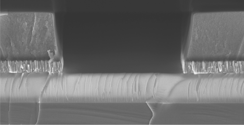 How this structure may actually appear upon SEM inspection.
This microstructure in turn can have a significant impact on film properties. For example, an open-voided structure would be more succeptible to oxidation throughout the film volume, yielding a much higher resistivity than the bulk metal. Choosing deposition conditions which achieve the desired microstructure and associated film propreties can therefore be a key consideration when developing a fabrication process flow—a choice made more easily when using our new Structure Zone Model Calculator, part of our nanoFAB Toolbox.
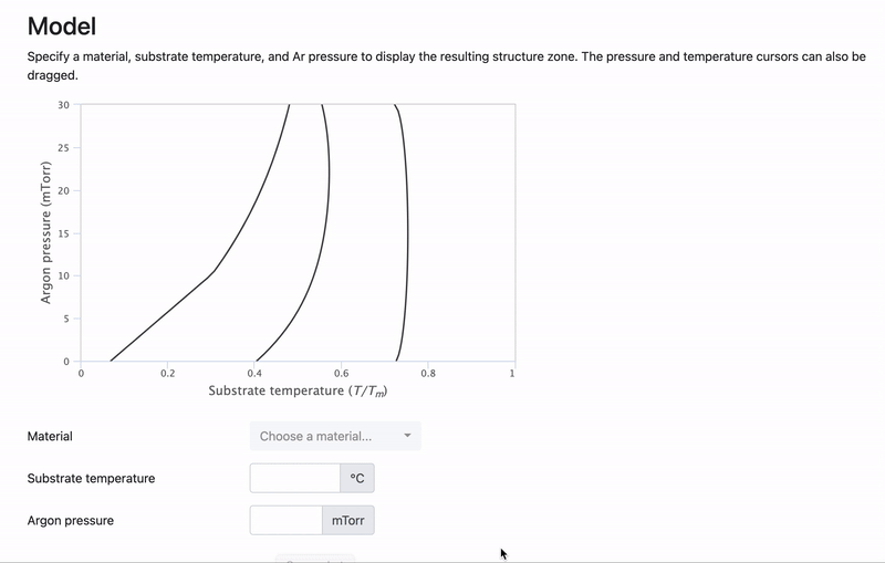
The Structure Zone Model (SZM) developed by J.A. Thornton defines four zones with qualitatively different microstructures, as a function of sputtering pressure and substrate temperature. Using our SZM calculator, the relevant zone can be quickly identified by specifying these two parameters, along with the material being sputtered. The cursors for pressure and substrate temperature may also be dragged to explore different regions of the sputtering parameter space. In either case, a description and diagram of the film morphology are displayed whenever the zone is well specified.
While we encourage all sputtering tool users to use this calculator to guide their choice of deposition parameters, there are a couple of caveats. First, please note that the zone boundaries are not sharp: being just inside a zone boundary does not guarantee that your film will have the archetypical characteristics of the zone in question. It is recommended to verify the film morphology directly using an imaging technique such as SEM for any critical work. Second, while we have included a large number of materials in the calculator, the presence of a given material does not imply that it is permitted to be deposited in any nanoFAB equipment (e.g., nobody will be allowed to sputter cesium at the nanoFAB in the foreseeable future). Finally, the sputtering tools at the nanoFAB are not necessarily capable of exploring the entire pressure–temperature space for a given material. In particular, only Sputtering System #2 (Doug) and Sputtering System #4 (Moe) are equipped with substrate heating at present.
If you have any questions about our new Structure Zone Model calculator or thin-film deposition at the nanoFAB in general, please do not hesitate to contact Aaron Hryciw (ahryciw@ualberta.ca).
Links
- Structure zone model calculator: toolbox.nanofab.ualberta.ca/szm