


Chromatic (Cc) aberration and Spherical (Cs) aberration are the two main factors limiting the ultimate spatial resolution that an electron microscope can achieve. The JEOL JEM-ARM200CF Atomic Resolution S/TEM at the nanoFAB Centre is equipped with a cold FEG source and a STEM probe Cs corrector to overcome these two aberrations. The cold FEG source produces an electron beam with an energy spread less than 0.3 eV (at 200 kV) to minimize Cc, while the STEM probe corrector generates a negative Cs coefficient to cancel positive Cs of the condenser lenses. The CEOS Cs corrector, which consists of two hexapoles and transfer lenses, corrects up to the 5th order Cs aberration, enabling a sub-Angstrom STEM probe with high current. This is critical for atomic resolution imaging and fast analytical probing at high spatial resolution. Below are atomic resolution images of nano-crystals, single atoms and epitaxial interface samples, obtained with High Angle Annular Dark Field (HAADF) STEM microscopy at 200 kV.
- Sample: Pd/Pt nano-crystals
User/Group: Chengcheng Rao / Prof. Jillian Buriak, Chemistry
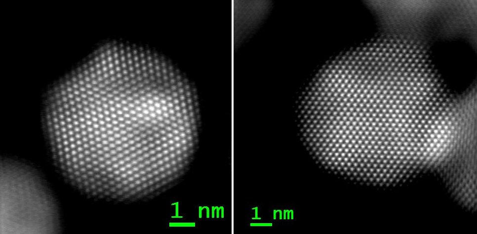
Cs corrected HAADF STEM images at 200 kV
- Sample: Ir Single atoms in carbon and MnOx matrix
User/Group: Dr. Bin Hua / Prof. Jingli Luo, CME
Detailed work can be found at J. Mater. Chem. A, 2019, 7, 23098-23104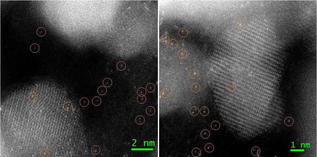
Cs corrected HAADF STEM images at 200 kV. Ir single atoms are highlighted in the circles.
- Sample: Cross section of Ga2O3 film on Al2O3 substrate
User/Group: Elham Borujeny / Prof. Ken Cadien, CME
Cross sectional TEM lamella was prepared on a ThermoFisher Helios G4 PFIB UXe DualBeam
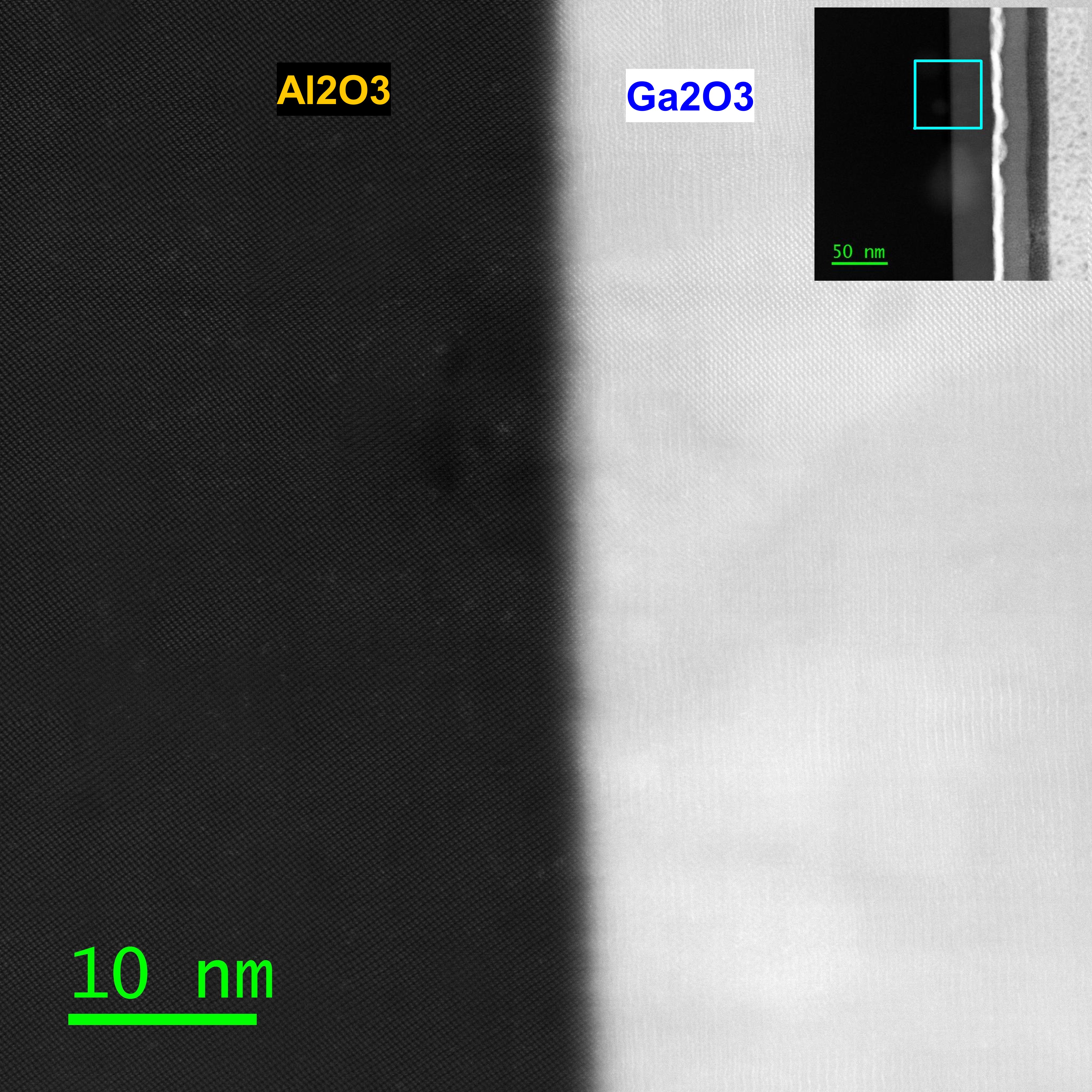
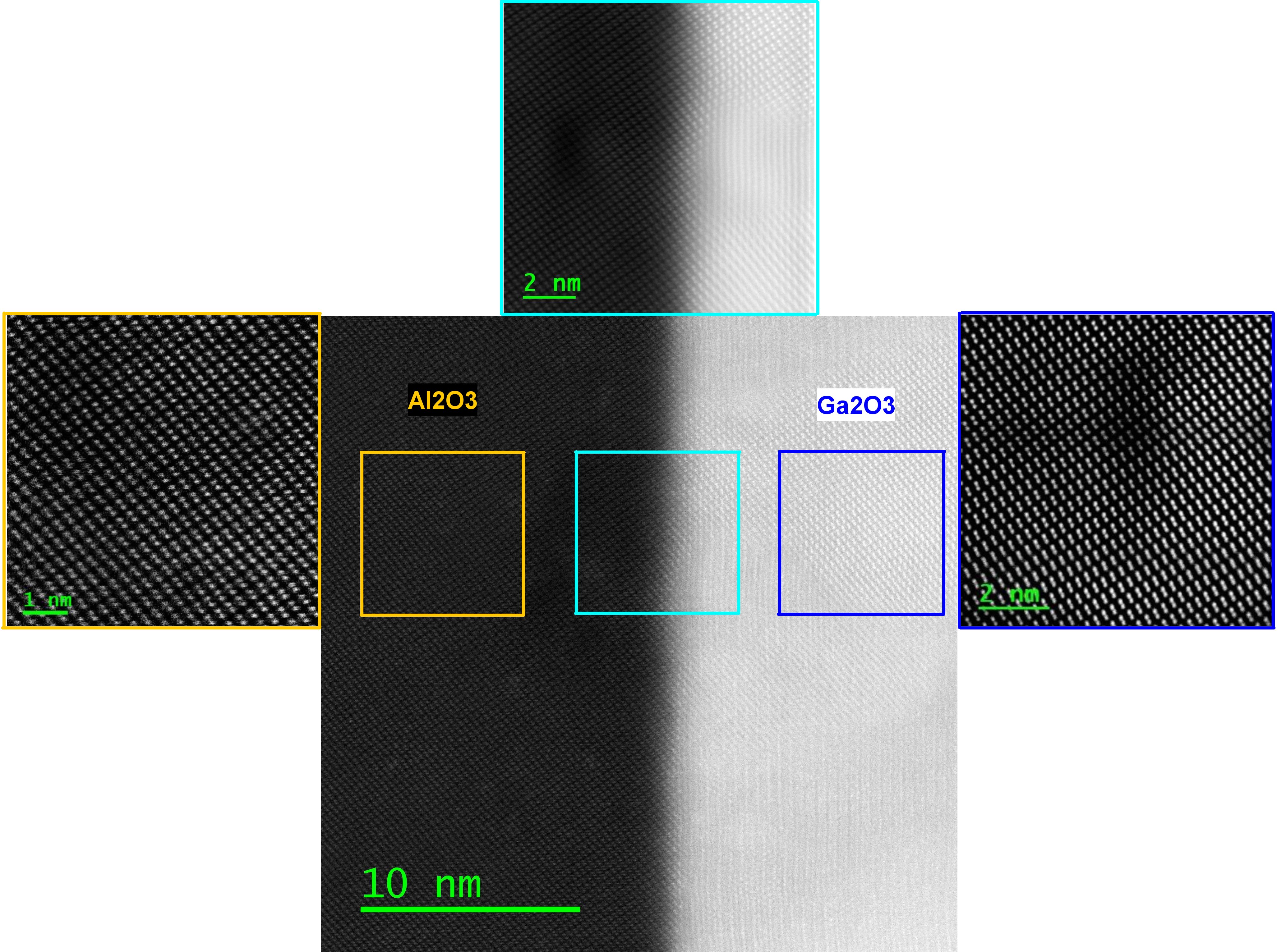
Cs corrected HAADF STEM images of Ga2O3 film, Al2O3 substrate and interfaces at 200 kV