


The nanoFAB is pleased to announce the winners of the 2019 nanoFAB Image Contest. Images were judged on criteria including image quality, technical merit, and overall aesthetic appeal, and voted on by nanoFAB staff members. This year, we also had our inaugural “Community Choice” award, with public voting. Congratulations to the winners, and many thanks to everyone who participated!
1st Place and Community Choice Award
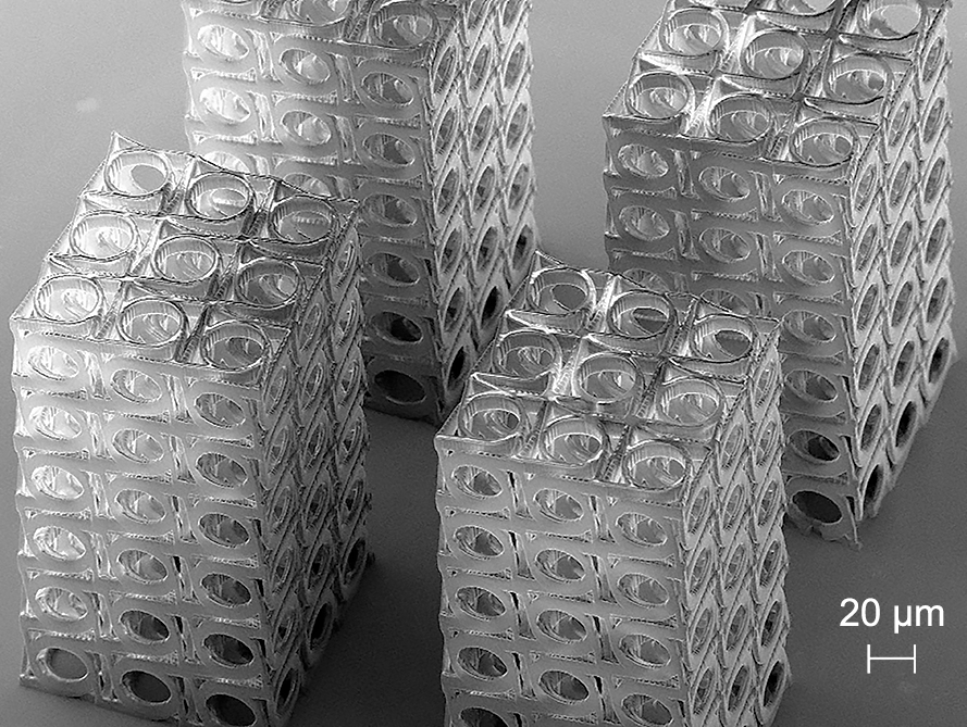
3D chiral mechanical metamaterial
Name: Joe Losby (Barclay Group, Department of Physics and Astronomy, University of Calgary and Freeman Group, Department of Physics, University of Alberta)
Description: The 3D chiral mechanical metamaterials exhibit the unusual property such that when compressed (from the top), the entire structure experiences a twist. This first-order coupling allows for transduction of a linear force through torque, or vice-versa. The acrylate-based structure was 3D printed using the Nanoscribe Photonic Professional GT and imaged with the Zeiss Sigma field-emission SEM. Special thanks to the inventors of the 3D metamaterial (cover feature, Science, Nov 24, 2017) and Gustavo de Oliveira Luiz for training and Nanoscribe exposure tips.
2nd Place
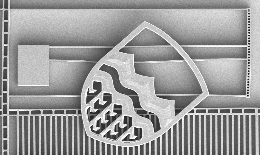
The University of Alberta logo on a MEMS comb drive resonator
Name: Mohammad Maadi (Zemp Group, Department of Electrical and Computer Engineering, University of Alberta)
Description: The image shows the University of Alberta logo on a micro-resonator after chemical etching of the silicon, fabricated during the ECE 457 lab.
3rd Place
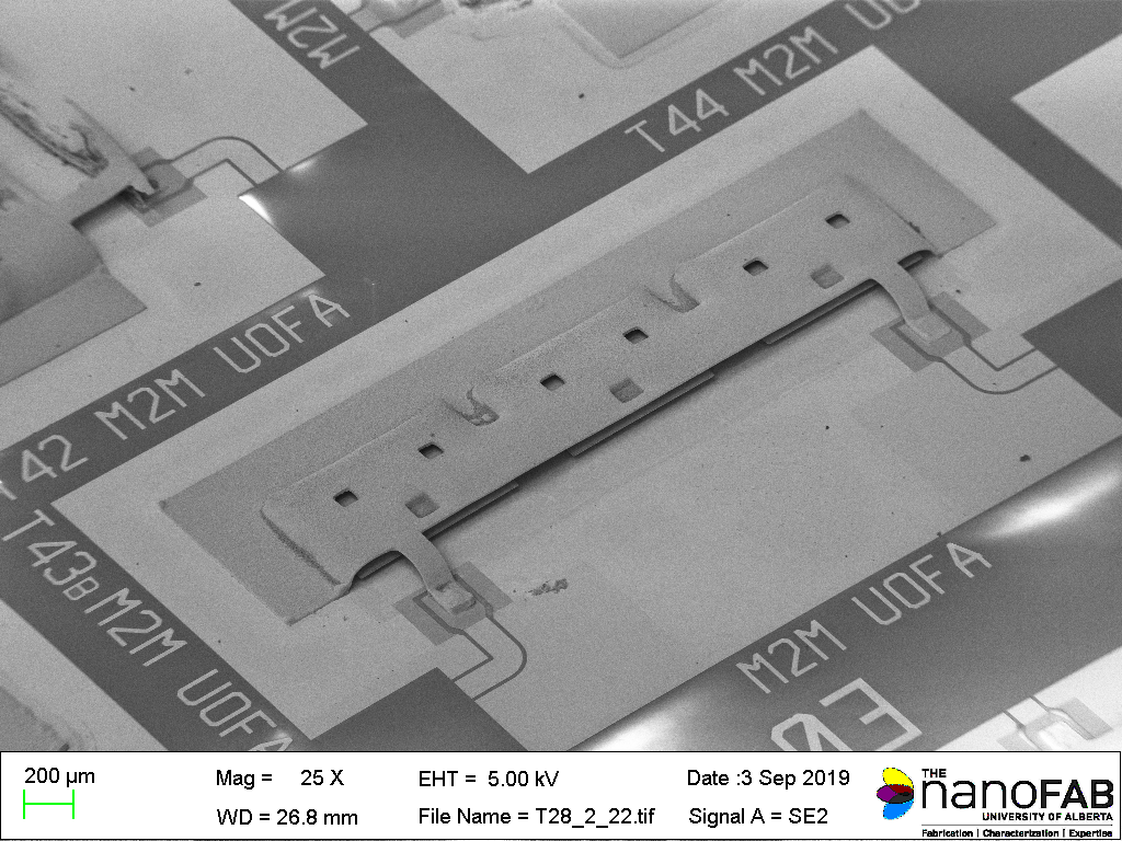
Miniaturized folded half-mode integrated waveguide cavity three-pole bandpass filter for 5G millimeter-wave communication systems in W-Band
Name: Tom Jones (Daneshmand Group, Department of Electrical and Computer Engineering, University of Alberta)
Description: This FESEM image shows a miniaturized three-pole integrated waveguide cavity bandpass filter for 5G millimeter-wave communication systems in W-Band. Using a folded half-mode technique, the footprint of the device is decreased by 91% compared to conventional integrated waveguide cavity, allowing more realistic integration with IC. The image was taken with the Zeiss Sigma FESEM at nanoFAB with the help of Dr. Anqiang He. The device itself was fabricated using a 5-mask lithographic process, with layers 25 nm thin up to 100 µm thick. The majority of the processes were completed in the nanoFAB, including photolithography using thin positive resist and chemically amplified AZ 40XT-11D thick positive resist, gold and copper sputtering and etching, and PECVD and RIE of nitride. The process allows for a three layer metallization stack, while the thick resist used to build the structure is removed at the end for air-filled cavities with no dielectric loss. Two 50-Ω ports feed the device, allowing for post-CMOS processing for technology integration.
Runner-up
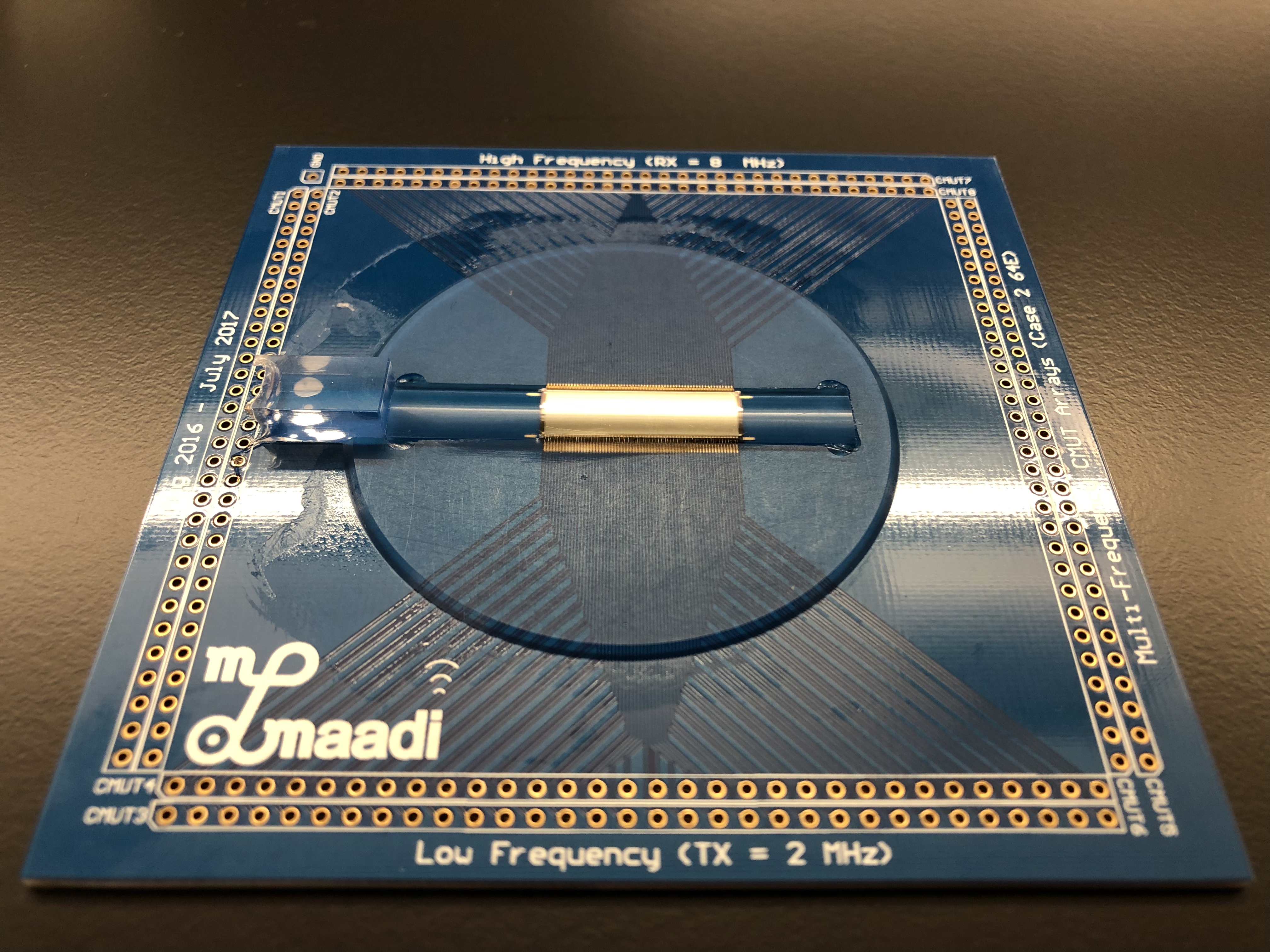
Large-scale multi-frequency CMUT array with ~50,000 ultrasonic transducers and an acoustic lens
Name: Mohammad Maadi (Zemp Group, Department of Electrical and Computer Engineering, University of Alberta)
Description: The figure shows a large-scale multi-frequency CMUT array with 128 sub-elements and almost 50,000 ultrasonic transducers. An acoustic lens was designed and fabricated on top of the array using PDMS to focus the beam on a focal point for ultrasound imaging purposes. These large-scale ultrasonic arrays were fabricated completely using the facilities at the nanoFAB. The arrays are then wire-bonded to custom PCB designs at NINT and finally become ready for ultrasound imaging unique applications. Multi-Frequency CMUT arrays require 6–7 lithography steps, HMDS, piranha cleans, thermal oxidation, BOE etch ing, KOH etching, critical point drying, RIE, PECVD, LPCVD, aluminum sputtering, and aluminum etching, along with more than 100 hours of work. These devices were characterized using the Filmetrics system, Alpha-Step IQ profilometer, Keithley semiconductor analyzer, Scanning Electron Microscopy (SEM), Laser Vibrometer, Zygo, Verasonics, Hydrophone measurement and the helium-ion microscope. The top side of the devices should be precisely protected during the KOH release of the silicon substrate and it should be possible to remove them without damaging the transducers.