The nanoFAB is pleased to announce the completion of Ga-FIB commission on the Zeiss Orion NanoFab Helium Ion Microscope (HiM). The Ga-FIB is open to user training now.
With the advanced nano-patterning and visualization engine (NPVE), the dual beam system (Ga and He) provides the user community with advanced capabilities and solutions to their fabrication and characterization application: (1) fast and sophisticated patterning with Ga-FIB; (2) hybrid fabrication with Ga and He beams; (3) sample preparation for internal structure characterization and (4) 3D FIB/HiM tomography.
If you have any questions and/or are interested to get trained on the HiM/Ga-FIB microscope, please contact Peng Li (Peng.Li@ualberta.ca).
Example works are listed below.
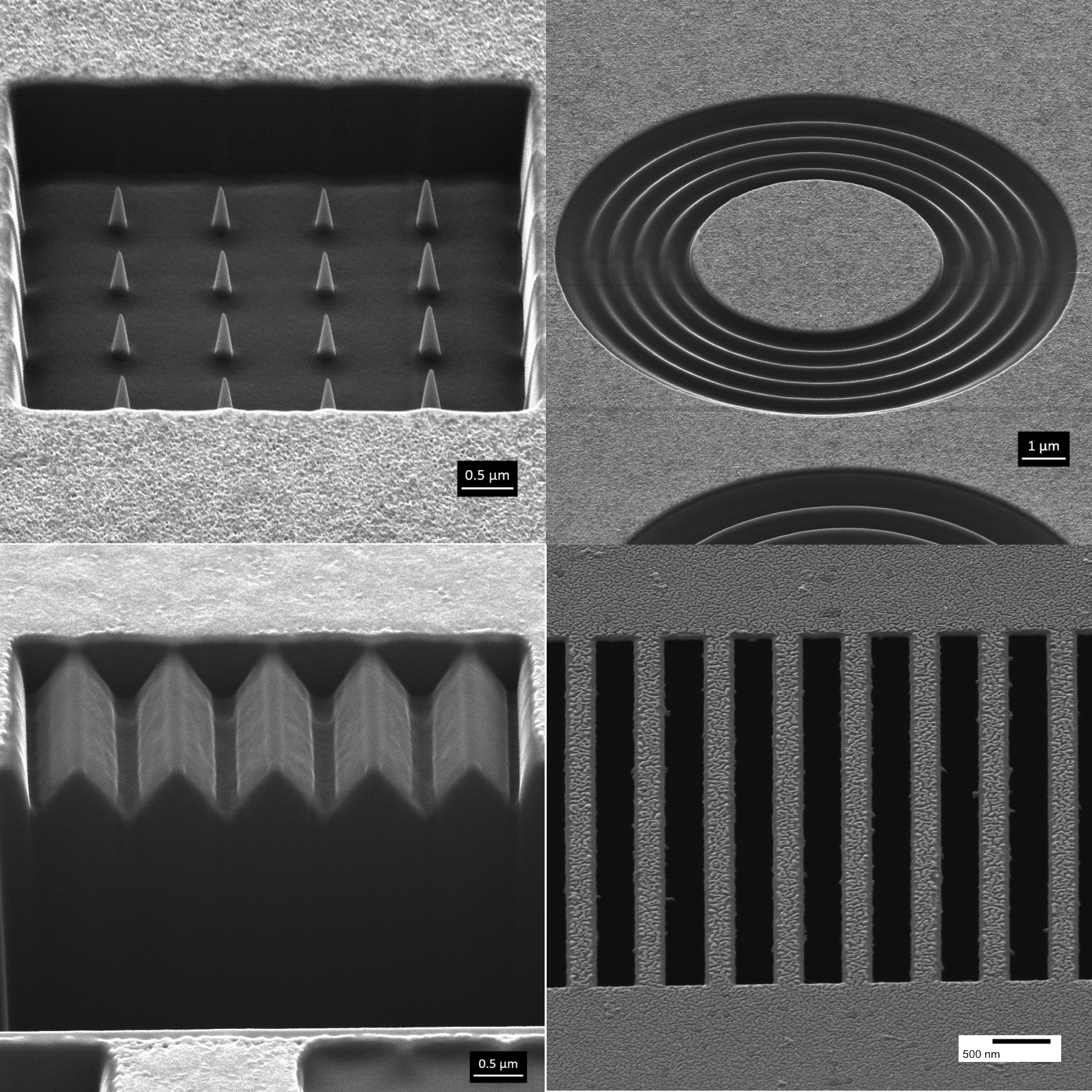
- Advanced Ga-FIB patterning:
3D Si nano-structure (upper left)
3D-profile on Si substrate (upper right and lower left)
Free-standing SiN gratings (lower right)
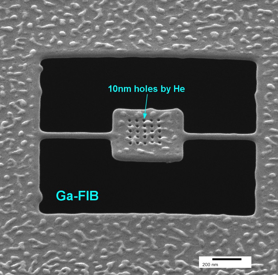
- Hybrid fabrication:
nano-pores milled (by He beam) into a SiN mechanical resonator (fabricated by Ga-FIB)
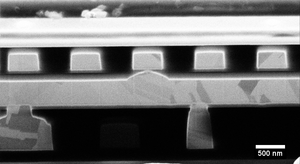
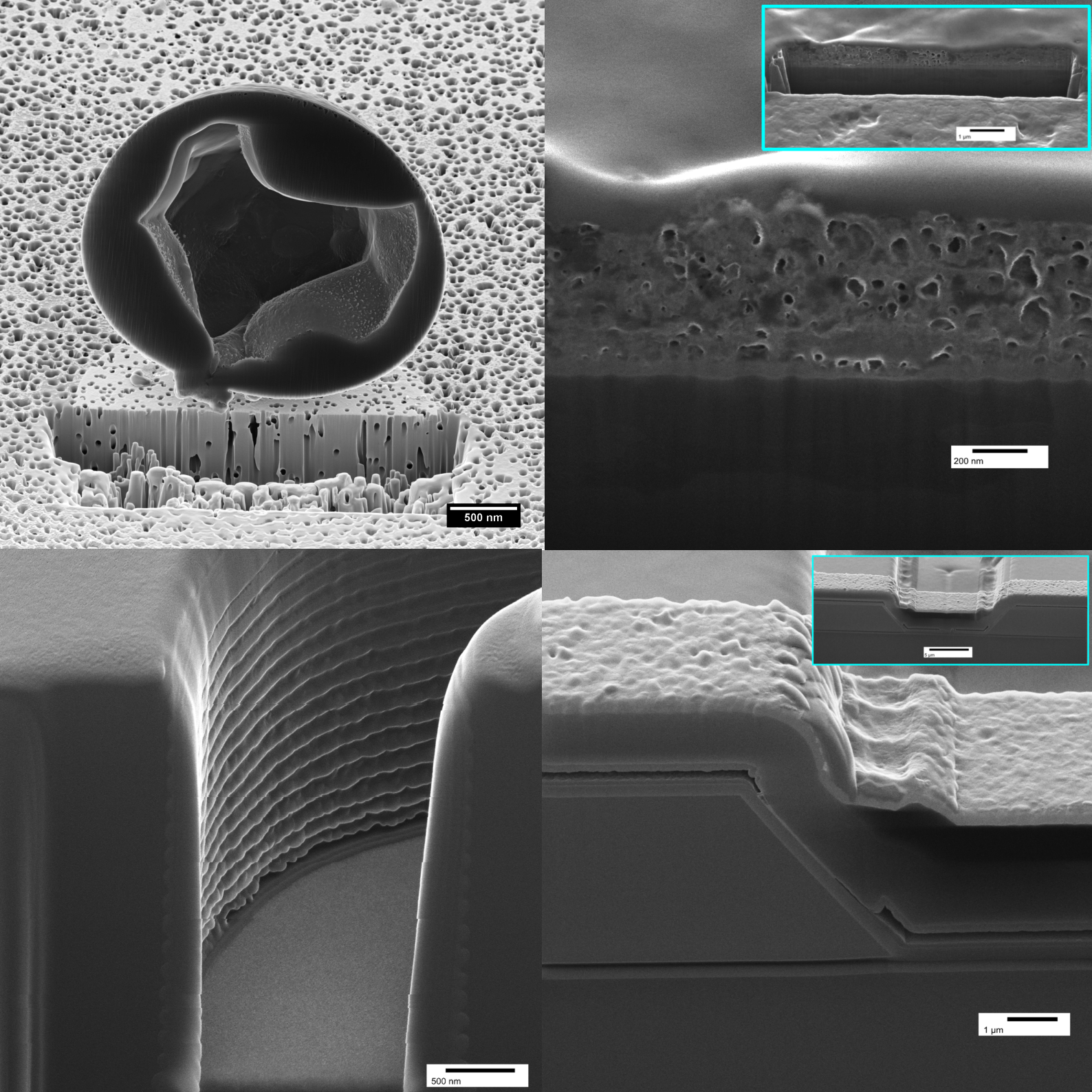
- Sample cross section (Ga-FIB):
Polymer bead (upper left)
Battery cell device* (upper right)
MEMS devices (lower left and right)
* This work is published in Nano Lett. 2015, 15, 6339−6348.
- 3D FIB/HiM tomography:
HiM image stack of a computer processor die
Movie Clip: tomo-processor-die