


The Zeiss Sigma FESEM at the nanoFAB has recently been upgraded with the following new capabilities:
(1) IBSS GV DS Asher: an in-situ chamber/sample cleaner
(2) Oxford LayerProbe: a non-destructive thin film thickness measurement software package
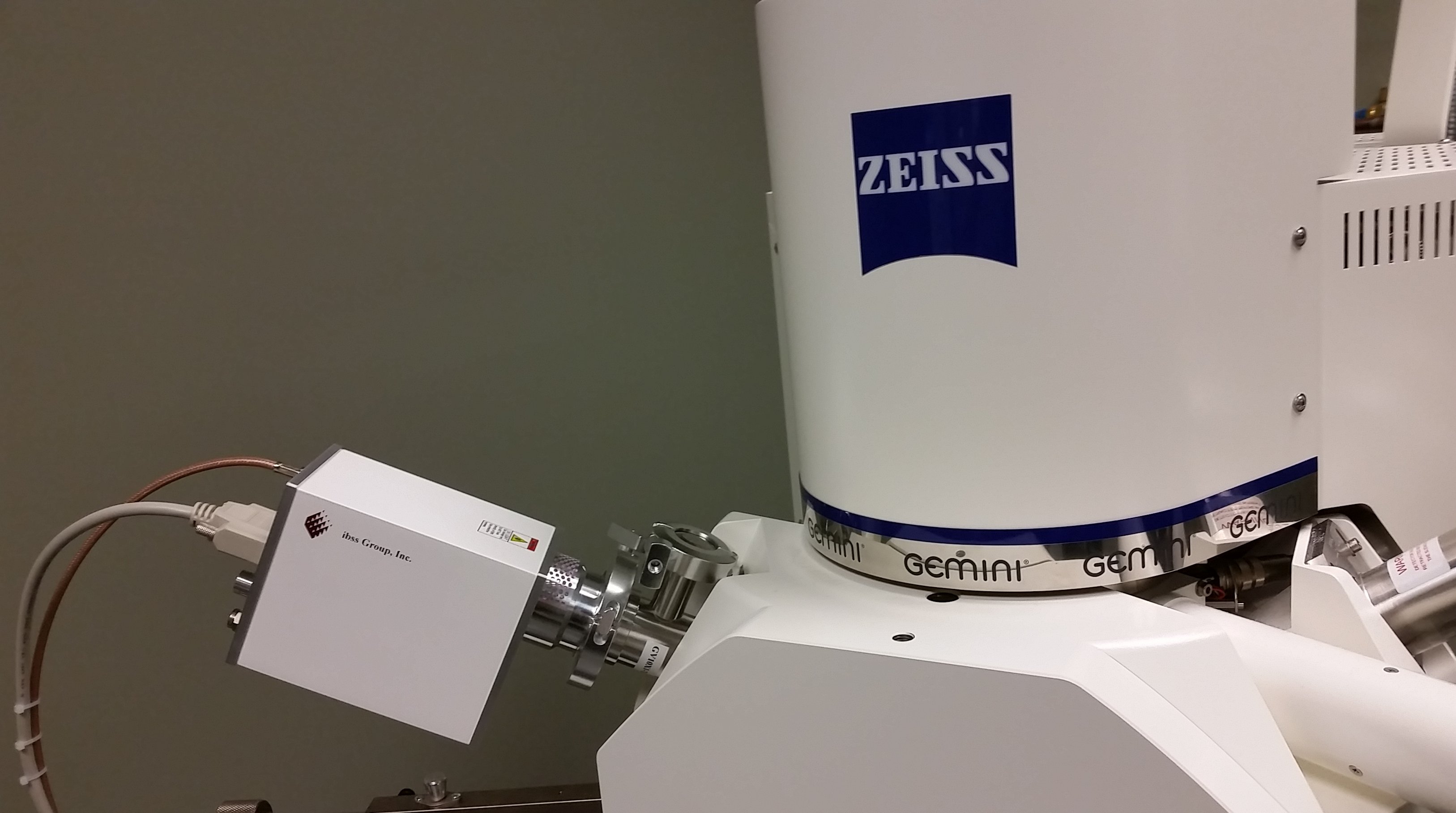
The GV10X Downstream Asher utilizes atomic oxygen and hydrogen to eliminates contamination by converting the surface carbon into gas phase molecules which are then pumped out of chambers – not just immobilized on. Being mounted on the microscope chamber, the cleaner provides capabilities of in-situ cleaning of both chamber and samples with very high cleaning efficiency and uniformity prior to imaging. With its extended pressure range, it allows continuously adjustable operation in the pressure range of <5 mTorr to 2 Torr (i.e. full operation with TMP on). The low operating power range (5-100 Watts RF Power) ensures no-damage to the samples (i.e. no heating, sputtering, or etching).
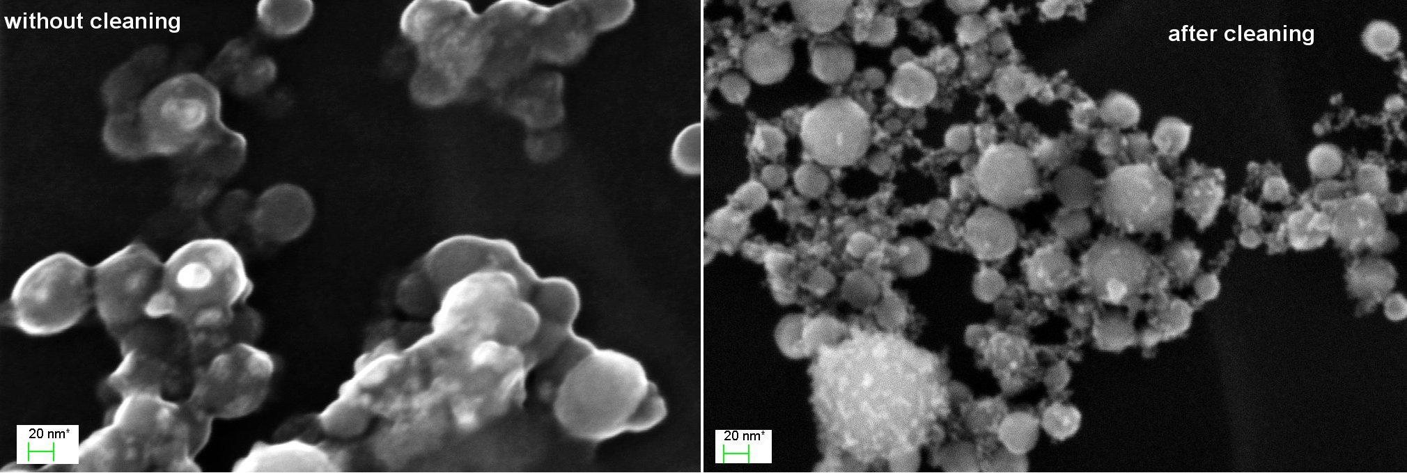
The images below show HR SEM images of Ceria coated Silica particles with and without cleaning. For details of the work, please see the paper tilted “Ceria coated silica particles: One step preparation and settling behaviour under the influence of colloidal and hydrodynamic interactions”, Materials Chemistry and Physics 173 (2016) 467 – 474, published by Prof. Ken Cadien Group, at CME department University of Alberta.
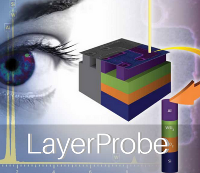
LayerProbe is an analytical tool for thin film analysis in the SEM, which is an add-on module to the Oxford AZtec EDS/EBSD microanalysis system.
LayerProbe complements the elemental and phase information gained from conventional EDS analysis by also calculating the composition and thickness of the individual layers beneath the surface.
Using a highly focused electron beam in an SEM to analyze a sample means the analysis is spatially resolved laterally as well as with depth, therefore nano-scale thin film structures can be measured.
Key features:
- Characterizes layer stacks
- Non-destructive analysis
- Thickness and composition of multiple layers from 2 nm to 2000 nm
- Lateral resolution down to 200 nm
- Easy to set-up for routine users
LayerProbe will be introduced in the upcoming MSC/Oxford workshop organized by the nanoFAB. Seminar is open to the public and registration is required for the hands-on demos. For detailed workshop information, please read the link here.
If you have any questions and/or are interested to test these new capabilities on the Sigma FESEM, please contact Peng Li (Peng.Li@ualberta.ca).